Micro-LEDs – Moving Day
Moving day is an intimidating process. Dozens upon dozens of boxes filled with your stuff, some of which dates back to High School or even earlier. There is some very important and sentimental stuff in those boxes. Your Farah Fawcett poster from your old room, your Magic the Gathering card collection, your signed “In-A-Gadda-Da-Vida” album from that night at The Whisky, and some of your wife’s less important stuff. The guys tossing those treasures into a van don’t grasp the significance of your stuff and are talking about some game they saw on the weekend while your stuff is carried around as if it were meaningless trash.
Just think what it would be like if you had to move 24,883,200 boxes, and each box was between the size of a red blood cell and a human hair? The good news is that Felix the mover could pick up thousands of those tiny boxes at one time and load them on the van, of course, he would have to be able to see them and not destroy them when he picked them up or when he put them in the truck, or when he took them out of the truck into their new home, but that is exactly what has to happen when constructing a micro-LED display.
Just think what it would be like if you had to move 24,883,200 boxes, and each box was between the size of a red blood cell and a human hair? The good news is that Felix the mover could pick up thousands of those tiny boxes at one time and load them on the van, of course, he would have to be able to see them and not destroy them when he picked them up or when he put them in the truck, or when he took them out of the truck into their new home, but that is exactly what has to happen when constructing a micro-LED display.
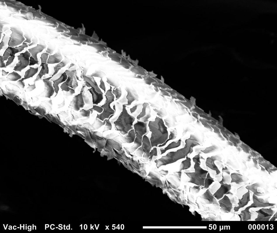
Hair Follicle - Source: Levy, Brian. “SEM Image of the Week: Only Their Hairdresser Knows for Sure.” Midwood Science.Org, 7 Nov. 2011, midwoodscience.org/?p=1136.
We did not just make up that 24.88m number, it’s the number of red, green, and blue micro-LEDs that would make up a full color 4K micro-LED display, and each of those 24.88m LEDs, is produced on one of three sapphire substrates, has to be picked up and placed on a substrate that will be the basis for the micro-LED display. So whose tiny fingers can do such a job? That’s a good question because there are a lot of companies trying to figure out ways in which to move these tiny LEDs, and revolutionize the display space.
The reason there is so much activity in the micro-LED space is that it has the potential to become a dominant display technology that could one day be as pervasive as LCD technology that began replacing CRT (Cathode Ray Tube) displays in the 1980’s. Notice we say ‘potential’ as there are some very difficult technology hurdles that have to be met before micro-LED technology can become more than a showroom oddity.
Aside from the necessity to solve a wide variety of technical issues, micro-LEDs do show promise, at least in a less than mass production setting, and compare favorably with both LCD and OLED technology, as shown in the table below, although we note that the source and circumstances of measurement of these characteristics can change the values considerably, and we note that brightness, measured on a cd/m2 basis is not a good indicator as to the viewers perception of a display’s brightness. That said, as a general comparison, it gives some idea why display manufacturers are willing to spend time and money to develop the potential for micro-LEDs.

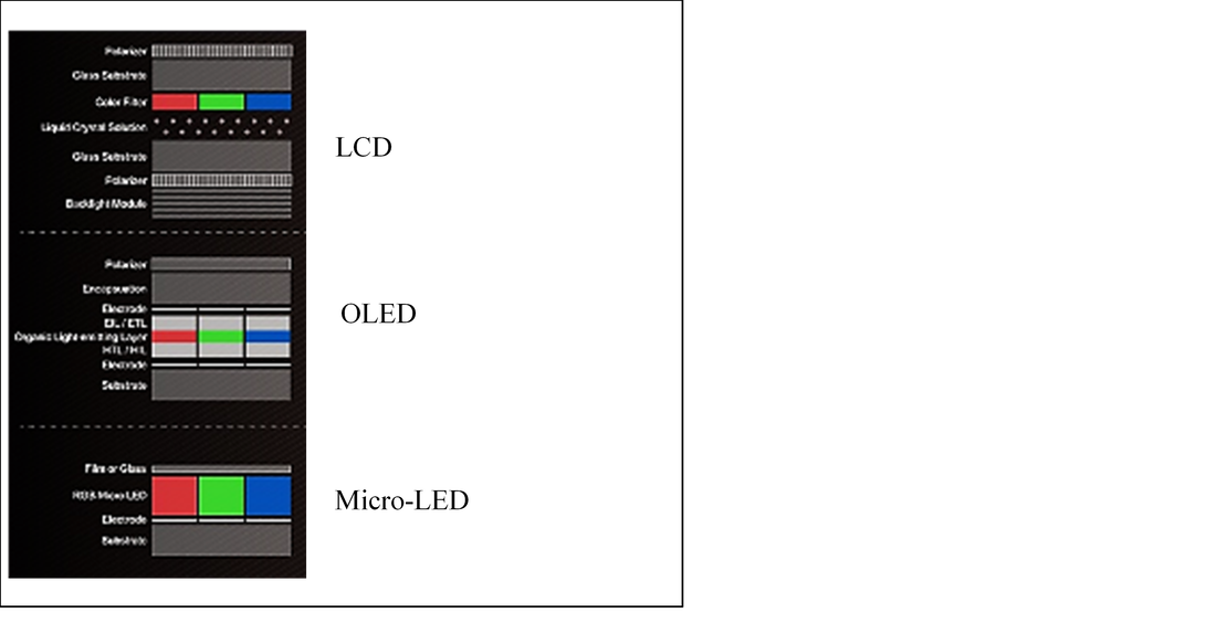
Display Structures - Source: Topway Display.com
Returning to our original thoughts about moving such small chips from wafers to a substrate, there are some other technical challenges that are keeping micro-LEDs from becoming a mass market product. As mentioned, the LEDs are small, but they are also of three different colors, red, green, and blue, and the materials used to make those LEDs are different, at least for red LEDs, which are based on Indium Gallium Phosphide (AlInGaP), while blue and green LEDs are both based on Indium Gallium Nitride (InGaN).. This means that each color LED has to be grown on a sapphire substrate in an MOCVD (Metal Oxide Chemical Vapor Deposition) tool, and then sliced into tiny die, and transferred and connected to a display substrate in a pattern that is typically horizontally spaced. The way in which this is accomplished is currently the biggest puzzle in the micro-LED saga, with almost as many ‘flavors’ as Baskin-Robbins (pvt), and we note the ‘connect’ part, which means that not only do the micro-LEDs need to be placed in RGB sequence, but the spacing and position much match the TFT driving circuitry to which each micro-LED is connected.
Typically larger LEDs can be connected to circuity via a metal wire that is soldered to a pad of conductive material, however that option is not available due to the large amount of substrate real estate it would consume, reducing the possible number of LEDs, along with the potential issues of what might happen to such thin metal wires during transfer and soldering. A more common method for connecting smaller LEDs would be flip-chip bonding, where a contact on the LED is bonded to a ‘bump’ of material that is in-turn bonded to the TFT driving circuit. This is certainly a more effective way to attach micro-LEDs to a substrate and TFT driver, but remember that this must be done almost 25m times for each display, and using current bonding tools, this can take many hours or even days, making the cost of production astronomical.
Typically larger LEDs can be connected to circuity via a metal wire that is soldered to a pad of conductive material, however that option is not available due to the large amount of substrate real estate it would consume, reducing the possible number of LEDs, along with the potential issues of what might happen to such thin metal wires during transfer and soldering. A more common method for connecting smaller LEDs would be flip-chip bonding, where a contact on the LED is bonded to a ‘bump’ of material that is in-turn bonded to the TFT driving circuit. This is certainly a more effective way to attach micro-LEDs to a substrate and TFT driver, but remember that this must be done almost 25m times for each display, and using current bonding tools, this can take many hours or even days, making the cost of production astronomical.

LED metal 'whisker' wiring - Source: https://www.nature.com/articles/s41377-020-0268-1/figures/7

Flip-Chip Bonding - Source: https://www.nature.com/articles/s41377-020-0268-1/figures/7
So, regardless of the speed at which micro-LEDs can be transferred, display engineers must consider the absolute accuracy of LED placement, which compounds the complexity of the transfer issue. But wait, there’s more… Even at the high rates of speed that specially designed pick and place tools can move micro-LEDs, there are some ‘in-between’ steps that complicate the process further. We noted that each of the three micro-LED colors are grown on a sapphire wafer, and while their small size allows for hundreds of thousands to be produced on a single wafer, each of those ‘smaller than the thickness of a hair’ chips needs to be ‘singulated’ (cut) from the wafer and must remain upright and in position to be ready for the transfer process. In some processes the micro-LEDs are transferred to a ‘tape’ that can be fed into a mechanical transfer system that places them on the display, but the time it takes to move the individual die to the tape must be included in the total production time, and that can be a time consuming intermediate process.
One way micro-LED engineers have come up with to eliminate that intermediate step is by using an Elastomer Stamp, a process championed by X-Celprint (pvt), that is said to be able to transfer 1m die/hr. The stamp is commonly made of PDMS (Polydimethylsiloxane), a silicon-based polymer that is used in shampoo to make your hair shiny. This material, or something similarly ‘sticky’ is pressed against a section of the singulated wafer and picks up hundreds of micro-LED die at once. The Stamp then moves to the display, where the stamp is slowly peeled back, leaving the micro-LEDs on the display substrate. This is an effective way to move large numbers of micro-LEDs, however the die must be pre-arranged to both match the receiving TFT pattern, and if it is an RGB display, they must be spaced to leave room for the two other color micro-LEDs, which then need to be transferred separately.
One way micro-LED engineers have come up with to eliminate that intermediate step is by using an Elastomer Stamp, a process championed by X-Celprint (pvt), that is said to be able to transfer 1m die/hr. The stamp is commonly made of PDMS (Polydimethylsiloxane), a silicon-based polymer that is used in shampoo to make your hair shiny. This material, or something similarly ‘sticky’ is pressed against a section of the singulated wafer and picks up hundreds of micro-LED die at once. The Stamp then moves to the display, where the stamp is slowly peeled back, leaving the micro-LEDs on the display substrate. This is an effective way to move large numbers of micro-LEDs, however the die must be pre-arranged to both match the receiving TFT pattern, and if it is an RGB display, they must be spaced to leave room for the two other color micro-LEDs, which then need to be transferred separately.
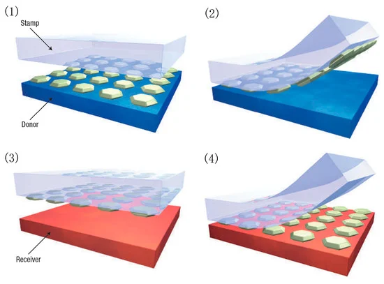
Elastomer Stamp Micro-LED Process - Source: https://www.mdpi.com/2076-3417/9/6/1206/htm
A small Korean start-up LC Square (pvt) has come up with what it believes is a way to modify the elastomer stamp process that will speed up and improve the accuracy of the transfer process. The die are removed from the wafer ‘en masse’ via laser lift-off and transferred to another wafer where the laser selects only those chips that match the correct location on what the company calls an ‘interposer’ with the process repeated for the other two colors. This creates a RGB pattern on the interposer which matches the TFT driver pattern on the display substrate.
The company then applies an ACF (Anisotropic Conductive Film) between the interposer and the display substrate and through heat and pressure, the ACF becomes the bond between the RGB patterned interposer and the TFT substrate, which allows the entire interposer to be placed at one time with all of the micro-LEDs in place and connected. LC Square provides either the three RGB interposers with chips, or the final interposer with all three colors placed, along with the ACF so it can be transferred by the panel producer. Of course, the practicality of such a process will depend on the cost, the metric all other transfer techniques are judged by, but the company insists that it can separate 1.2m micro-LED chips from wafers and create an interposer in 4 minutes, with a placement accuracy of +/-2µm at a yield of 99.99%.
One possible solution, interim or otherwise, is to use a single color blue micro-LED for all sub-pixels and use quantum dots to convert blue to red and green in 2/3 of the sub-pixels. While this is similar to the way LG Display (LPL) produces large panel OLED TVs, the use of quantum dots would eliminate the brightness loss that reduces OLED TV brightness when using phosphor based color filters. Quantum dots do not block other colors as phosphors do, but shift the wavelength (color) of the light in a highly efficient manner, and the creation of a quantum dot color filter could be accomplished using ink-jet or similar mass production technology. Such an idea solves the problem of selective placement of RGB micro-LEDs, but still leaves a big open issue as noted below.
Again we note that there are quite a few other technologies being explored in relation to producing micro-LED displays, but our look at just one technology and a variant, points to not only how much research is being done in the area of micro-LEDs, but just a few of the challenges facing the commercialization of the technology. Each new system has to face not only the question of speed but the even bigger question of what to do with those micro-LEDs that do not work once they have been placed. Even with an accuracy of 99.99%, a 4K display would have 2,489 micro-LEDs that do not work and would have to be removed and replaced, a far more arduous task than the initial placement, which would likely cost as much or more than the transfer process itself. More to come.
 RSS Feed