The Micro-LED Parallel: Solving the CPO Power Crisis with Display-Grade Technology
Remember Micro-LEDs? They are the stuff of high-resolution displays that cost correspondingly high numbers, reaching into the hundreds of thousands of dollars. Only a short few years ago they were going to revolutionize the display industry and replace both LCD and OLED displays with brightness levels unable to be generated with any other display technology. As with most technology, the practical application is typically much more difficult than the hype and while Micro-LED display technology is still being developed and occasionally hits the retail market in some form, it has proven more difficult to manufacture than originally expected.
The problem is that Micro-LEDs are small, very small, and are typically grown on a layer of Gallium Nitride on Sapphire. Once grown they must be removed from the wafer and transferred to a substrate, typically glass or PCB. As there are three (R,G,B) sub-pixels for each pixel in a display, a 4K TV requires roughly 8.3 million pixels or almost 25 million micro-LEDs. To make things even more difficult, red Micro-LEDs are grown from a different material than blue and green Micro-LEDs, so moving the Micro-LEDs from their growth wafers to a substrate means picking LEDs from at least two wafers. Using a laser to lift off the Micro-LEDs from the growth wafer is now the industry standard but yield is also a major factor that can temper the advertised speeds of current transfer equipment.
We note that while peak transfer speeds of 100 million to a billion Micro-LEDs/hour are advertised, the reality is that actual throughput is closer to 20 million transfers/hour, or a bit less than one 4K display. An LCD 4K display comes of a mass production line roughly every 15 seconds, which points to why the cost of Micro-LED displays remains high. Yield is also a consideration as even Five nines of accuracy for Micro-LEDs yields roughly 2,500 dead pixels per 4K device.
Does this mean that Micro-LEDs are not viable for displays? Not really, as the display industry continues to make improvements in each of the key Micro-LED processes, but it does push out Micro-LEDs as a display application that can compete with LCD and OLED for a few more years.
The Shift to AI Infrastructure
So why spend time on Micro-LEDs? Because there is another application that promises to breathe life into Micro-LEDs and (ta-da) it is associated with AI and looks to be much more “immediate” as a practical application. The application, known as Micro-LED Co-Packaged Optics (CPO), is a substitute for copper cables and traces that act as interconnects between server racks and network switches in data centers. Copper DACs still dominate the market, at between 45% and 50% of new port installations, especially for short (>1.5m) connections, and Linear Pluggable Optics (LPO) are running 2nd at 25% to 30% of new port installs, but CPO is the most rapidly growing technology and represents the top of the technology chain.
Here is how it works:
In typical silicon photonics a laser generates the ‘carrier light”, sort of a dial tone. These lasers are external devices and remain “on” at all times. This means the power consumption is predictable as is the wavelength (usually 1311nm). In order to keep the 700 Watts of heat generated by the GPU from damaging the laser, it is housed in a separate module and pipes the light into the optics that are packaged with the GPU. The GPU data triggers the CPO and the external laser transmits the modulated light down the fiber. At the other end, the light is translated back to an electrical signal.
This works well but presents challenges:
So, if CPO has so many drawbacks, why use it?
Here’s where things have changed. CPO 2.0 is based on Micro-LEDs instead of lasers. Micro-LEDs are much more thermally stable than lasers. Stable up to 125°C while lasers need isolation and cooling. Both lasers and Micro-LEDs are difficult to repair but Micro-LEDs last longer. As lasers are always on they require power at all times. Micro-LEDs only require power for the time they are on and that time is a short pulse.
The problem is that Micro-LEDs are small, very small, and are typically grown on a layer of Gallium Nitride on Sapphire. Once grown they must be removed from the wafer and transferred to a substrate, typically glass or PCB. As there are three (R,G,B) sub-pixels for each pixel in a display, a 4K TV requires roughly 8.3 million pixels or almost 25 million micro-LEDs. To make things even more difficult, red Micro-LEDs are grown from a different material than blue and green Micro-LEDs, so moving the Micro-LEDs from their growth wafers to a substrate means picking LEDs from at least two wafers. Using a laser to lift off the Micro-LEDs from the growth wafer is now the industry standard but yield is also a major factor that can temper the advertised speeds of current transfer equipment.
We note that while peak transfer speeds of 100 million to a billion Micro-LEDs/hour are advertised, the reality is that actual throughput is closer to 20 million transfers/hour, or a bit less than one 4K display. An LCD 4K display comes of a mass production line roughly every 15 seconds, which points to why the cost of Micro-LED displays remains high. Yield is also a consideration as even Five nines of accuracy for Micro-LEDs yields roughly 2,500 dead pixels per 4K device.
Does this mean that Micro-LEDs are not viable for displays? Not really, as the display industry continues to make improvements in each of the key Micro-LED processes, but it does push out Micro-LEDs as a display application that can compete with LCD and OLED for a few more years.
The Shift to AI Infrastructure
So why spend time on Micro-LEDs? Because there is another application that promises to breathe life into Micro-LEDs and (ta-da) it is associated with AI and looks to be much more “immediate” as a practical application. The application, known as Micro-LED Co-Packaged Optics (CPO), is a substitute for copper cables and traces that act as interconnects between server racks and network switches in data centers. Copper DACs still dominate the market, at between 45% and 50% of new port installations, especially for short (>1.5m) connections, and Linear Pluggable Optics (LPO) are running 2nd at 25% to 30% of new port installs, but CPO is the most rapidly growing technology and represents the top of the technology chain.
Here is how it works:
In typical silicon photonics a laser generates the ‘carrier light”, sort of a dial tone. These lasers are external devices and remain “on” at all times. This means the power consumption is predictable as is the wavelength (usually 1311nm). In order to keep the 700 Watts of heat generated by the GPU from damaging the laser, it is housed in a separate module and pipes the light into the optics that are packaged with the GPU. The GPU data triggers the CPO and the external laser transmits the modulated light down the fiber. At the other end, the light is translated back to an electrical signal.
This works well but presents challenges:
- Heat – CPO requires that the laser be near the GPU. This causes the laser wavelength to drift. Too much drift and the receiver cannot “see” the data.
- Power – Lasers are always on and maintain a carrier signal even when no data is flowing which means it is power inefficient.
- Sensitivity – Lasers are sensitive to heat and need thermal protection
- Complexity – Lasers require separate ‘modulators’ that add to complexity.
So, if CPO has so many drawbacks, why use it?
Here’s where things have changed. CPO 2.0 is based on Micro-LEDs instead of lasers. Micro-LEDs are much more thermally stable than lasers. Stable up to 125°C while lasers need isolation and cooling. Both lasers and Micro-LEDs are difficult to repair but Micro-LEDs last longer. As lasers are always on they require power at all times. Micro-LEDs only require power for the time they are on and that time is a short pulse.
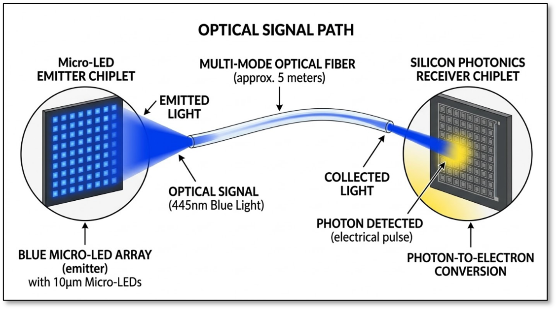
Figure 3 - CPO 2.0 Signal Path - Source: SCMR-LLC, Nno-Banana
Furthermore, Micro-LEDs are simple and do not require a separate modulator, and while lasers must be aligned to a 9um single mode fiber, Micro-LEDs are able to use 50um multi-mode fiber, making the alignment process considerably easier. Lasers run “Narrow & Fast” meaning they run at 100Gbps per lane which generates large amounts of heat. Micro-LEDs run “Wide & Slow”, ~2-4Gbps across thousands of lanes., essentially parallel processing the data. The bottom line is that most drawbacks of lasers in this environment are opportunities for Micro-LEDs.
Right now, CPO 2.0 (Micro-LED) is more expensive than CPO 1.0 (laser) on a per link basis, but that premium is the result of a more mature laser supply chain and will diminish over time, with estimates for late 2027 as the point at which it will be cheaper to produce CPO 2.0 than CPO 1.0 when including yield improvement.
But it doesn’t end there. A standard 1.6T laser based module consumes ~30 Watts of power. That same equivalent link using CPO 2.0 (Micro-LED) consumes ~1.6 Watts. Using the example of a 100,000 GPU cluster, moving from CPO 1.0 to 2.0 saves approximately 15 million kWh per year, which comes to a savings of ~$1.5 million per cluster. Additionally the cooling cost of CPO 1.0 is significantly higher than 2.0. Lastly the cost of multi-mode fiber is roughly 40% cheaper than single-mode, adding to the cost savings for 2.0 over time, so over a 5 year period, while the 2.0 install cost $1,000 more than 1.0 the energy savings over that period would give the 2.0 install a $5,000 per port advantage.
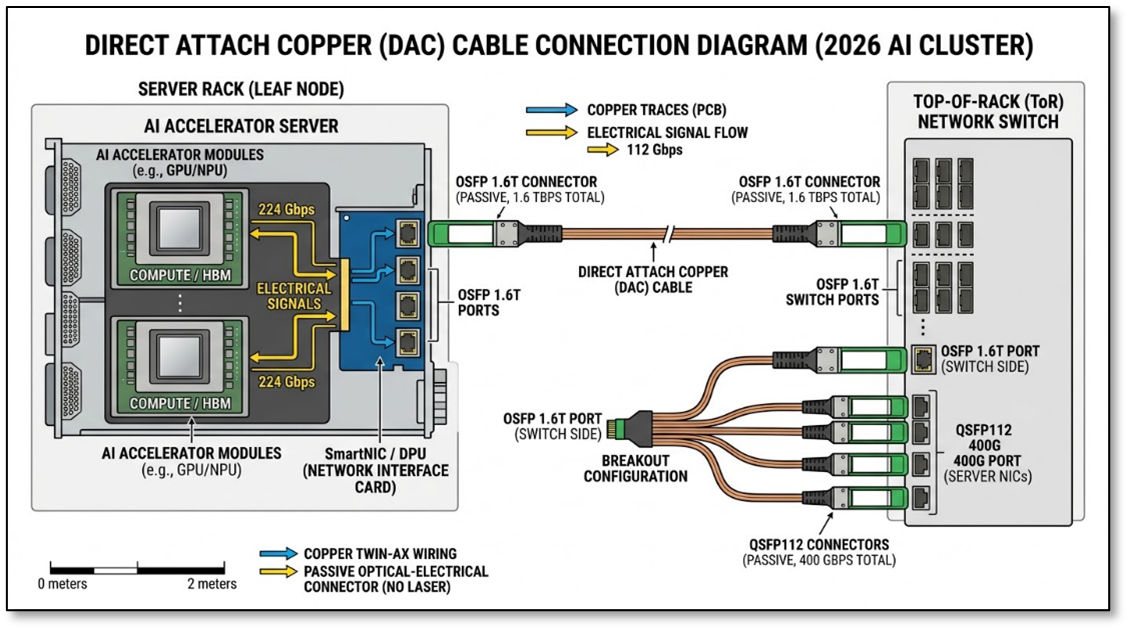
Figure 1 - DAC Cable Connection Diagram - Source: SCMR-LLC, Nanao-Banana
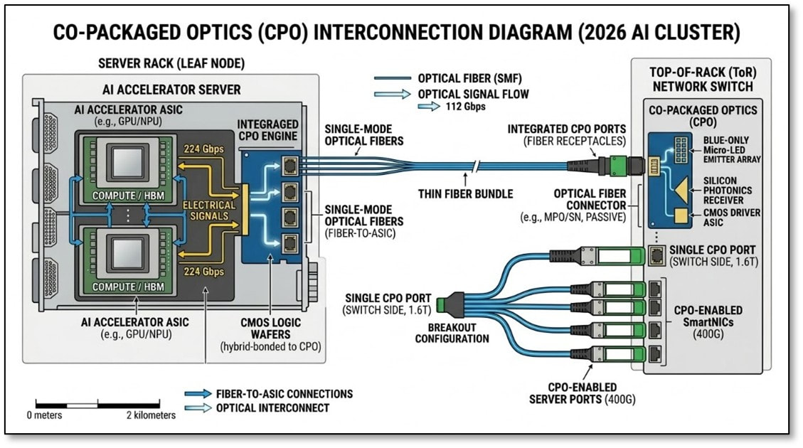
Figure 2 - CPO Optics Interconnection Diagram - Source: SCMR-LLC, Nanao-Banana
Conclusion: The Diversification of Micro-LED and the End of the ‘Carrier’ Era
The evolution of Micro-LED from a high-end display prospect to a critical AI infrastructure component represents a fundamental shift in how we think about the energy-per-bit required to fuel the AI revolution. While the display industry continues to refine the massive transfer processes required for consumer screens, the data center has provided an immediate, high-value application that bypasses those scale barriers. This transition from CPO 1.0 to 2.0 is more than just a component swap; it is a permanent shift in the economic calculus of high-speed networking.
As of March 2026, the landscape has changed. With the signing of the Ratepayer Protection Pledge at the White House this month, the era where Big Tech could socialize the cost of inefficient energy use has ended. Hyperscale’s are now directly responsible for every megawatt of new generation they require. In this "pay-to-play" energy landscape, the 10-month break-even period of Micro-LED optics isn't just a competitive advantage—it’s a survival requirement.
By moving from the "Narrow & Fast" carrier-based laser models to the "Wide & Slow" parallel architecture of Micro-LEDs, data center operators are finally scaling past the thermal and financial limits of silicon photonics. Micro-LED may still be the future of the living room, but today, it has found its true calling as the essential, invisible nervous system of the global AI economy—proving that the most disruptive innovations often find their greatest success in the places we least expect them.


 RSS Feed