VT vs. FIN
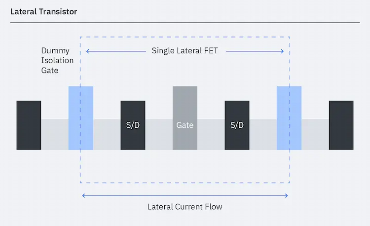
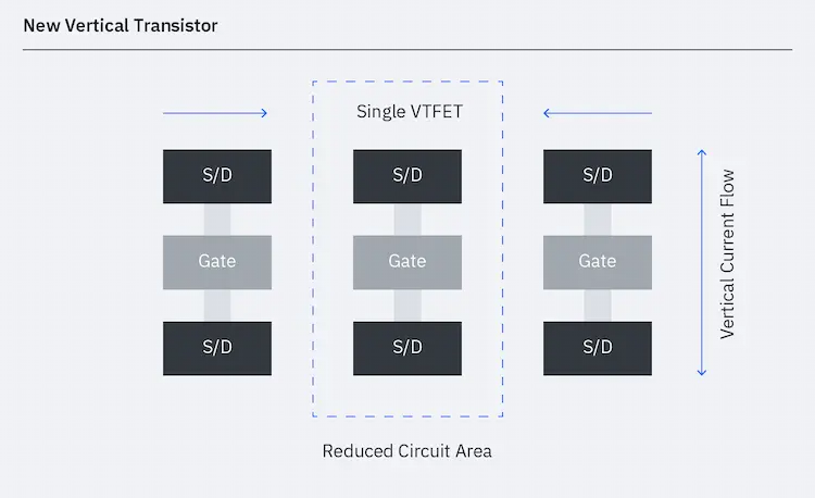
“We will control the horizontal. We will control the Vertical”. Such were the words of the ‘control voice’ before every episode of the 1962 Sci-fi series “The Outer Limits”, but it seems they are again apropos to the semiconductor space where a joint development effort between Samsung Electronics and IBM (IBM) has developed a way in which the fragility of Moore’s Law can be challenged. The device type is called a VTFET (Vertical Transport Field-Effect Transistor) as opposed to the common FinFET (Fin Field-Effect transistor), where transistor gates are places around the transistor source and drain, both to allow the circuit to be opened or closed, but also as ‘dummy’ gates to isolate the cell from others. As FinFETs are laid out horizontally on a silicon wafer, those dummy gates and interconnect wiring all take up room, limiting the density of FinFET devices as per Moore’s Law.
Samsung and IBM have found a way to stack source, drain, and gate structures in order to further increase the number of transistor cells on a wafer. According to both companies, the technology will allow for two times the performance of current FinFET technology and up to an 85% power savings without reducing the space (pitch) between each transistor, which also reduces the distance power has to travel and the distance between vertical cells, which improves performance, along with the ability to be less constrained as to the size of each sorce, drain, and gate structure.
All in, this is a step toward another iteration in the ability to produce circuitry that is required for faster and more complex computing, without the issues facing sub-nanometer node production. Neither company has set a timetable for products using the technology, but we would expect early versions to be shown next year, although real implementation will likely take a few years to further define production processes. It is certainly a step forward in IC design.
Lateral Transistor Structure - Source: IBM
Vertical Trasistor Structure - Source: IBM
 RSS Feed