Data, Data, Data
Over the last few months we have been researching the potential for the advancement of automation in the semiconductor space, meaning the ability of a semiconductor fab to self-correct as silicon moves down the process line, with the ultimate purpose being to increase yield. As part of the research we have found that such a system, and even systems currently in place, would not be limited by a lack of data necessary to make such corrections in-process, but quite the opposite. In most fabs, and even in much less complicated production processes, there is too much data, a result of smaller and more accurate sensors that can be placed in more locations with better sensor measurement capabilities and faster data collection networks.
We have found that while there are some data standards that span a number of semiconductor processes, it is the job of process data engineers to look at data generated from each piece of equipment in order to analyze where the line is facing issues, and this could mean data from many sensors on each process tool. As data collection sensors have improved and collection points increased, the amount of data that needs to be reviewed has become overwhelming, to the point that it can be a hindrance rather than a help.
One vivid example was shown to us concerning a relatively simple process in the CE world, solder reflow inspection on PC boards, a process where the board is pre-heated, solder paste[1] added, and then cooled, which attaches components to the PC board. While reflow is a basic process that has evolved over the years, typical problems that occur during reflow, such as component shift or delamination of the board, can not only cause the board to be pulled off the line for further inspection (and cost), repair, or to be scrapped entirely, but can become a source of serious problems when the boards reach customers in products.
In many cases PCB boards are inspected visually as they pass through a line, although humans are easily distracted or fatigued, leading to the use of AOI (Automated Optical Inspection) tools that use image sensors to match a board’s captured image to a stored template. However even AOI tools are subject to errors, particularly false defects, which can be caused by light reflection or other optical interference, which pushes more sophisticated PCB lines to use tools that perform a number of measurements in addition to template matching as the boards pass through the production line.
One example we saw was a system that was evaluating PCB boards that were ~8.3” x 6.3”, a bit more than half the size of a sheet of paper. The tool measured height, width, and area at over 3,400 points on the board and checked for x/y offset (components that were placed incorrectly during reflow), generating 17,000 data points for each board. The data was fed to SPC (Statistical Process Control) software, which, in theory, is supposed to correlate the data, allowing a process engineer to track back where defects were being generated in order to make corrections to the line.
What was most surprising was that in many cases, when a board was flagged by the system, the process engineer let the board remain in the line, under the theory that the final AOI and SPC review would pull the board before it was shipped. This defeated the purpose of the entire system as the flagged board continued to be processed, despite the fact that it had defects and would either need repair which could entail removing later process steps, or could be scrapped entirely, and if the defect was not clarified and the reflow process fixed, it could continue to affect subsequent boards. When asked why the engineer let the flagged board go through, the comment was that there are so many data points that the chance for false negatives continues to increase with the number of measurement points, so rather than pull the board they left the determination up to the final inspection engineer, essentially defeating the purpose of the data collection early in the process line.
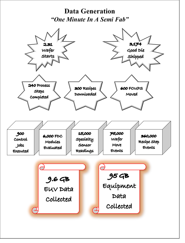
While this was an example using a relatively simple process and tool set, producing semiconductors is far more complex, with memory producer Micron (MU) stating that it takes more than a thousand process and measurement steps to produce modern chips. To put just the feature size of those structures into perspective, think of a chip die, typically about the size of a fingernail, being blown up to the size of a football field. Take one blade of grass from that field, cut it in half, cut it in half again, and cut it in half a third time. That’s the size of one transistor, essentially one bit of storage, out of the 8 billion on a typical memory chip, so the amount of data generated by tools to make sure things are where they should be on semiconductors is enormous, more than all the data collected by Facebook (FB), Amazon (AMZN) and all the other social media companies, although over 80% of it is not ever looked at by process engineers.
Most semiconductor process engineers are only interested in data when there is an ‘excursion’ in the semiconductor fabrication process, a nice way of saying ‘an error’, as these can cause millions in losses considering the number of die on each wafer and the number of wafers processed each hour. Some semiconductor customers require (military, automotive) that the data be stored for up to 15 years, even if it has never been reviewed, but ~90% of the available semiconductor process data is less than two years old according to T&M companies, which means the amount of data being generated during the last few years has increased dramatically.
So the question then becomes whether it is actually helpful to add sensors, data collection points, and sample rates if most of the data is never going to be used? The fear that at some point the data might be useful pushes the industry to collect everything, even if it seems unnecessary, ‘just in case’, but does it really help to improve yield, the ultimate goal, if most of the data is ignored? Not really, so improving sensors, adding data collection points, and increasing data collection network speeds all sound good on paper but the increases in process data volumes don’t seem to lead to large gains in productivity and yield, so where is the problem?
The problem is that humans are not interested in the data as a whole, only if it solves an immediate problem, while computers are designed to process data, especially large amounts of data, and can be ‘trained’ to spot even the smallest anomaly. This is essentially what SPC software is supposed to do, help a human engineer spot a problem and trace it back to its source, a process that even in the PCB example above, would entail the engineer having to look at the data from a number of tools in order to spot the root cause of the error, something that computers can do far more easily than humans, and if we trusted the computer, we could actually let the computer make the necessary adjustments to the process tools without getting involved.
This is the goal of semiconductor foundries; to fully automate the process using a self-correcting system that could make corrections on a tool-by-tool or process by-process-basis, leaving the human engineering staff to come up with better and more efficient process steps. Unfortunately there is a problem, and that comes back to the data. Much of that data is collected at the tool level and tool manufacturers want users to be able to use that data through a platform specific to that tool while the next tool vendor wants the user to use his platform for the data, leading to lots of data that is not uniform, especially as tool vendors and the industry overall is just coming to the conclusion that the amount of data is so vast that AI and machine learning systems are the only way in which the data can be utilized. This leads to the conclusion that the data must be uniform and organized to avoid the need to ‘clean’ the data or reformat same before it can be processed, which puts bottlenecks into the potential feedback loop.
There are some tools that are self-correcting, such as ASML’s (ASML) EUV tools that allows the tool to measure and compensate for sub-nanometer inaccuracies that occur as the scanner operates, feeding back that measurement data directly to actuators at the reticle stage, which compensate for those minute changes that would otherwise become potential excursions. ASML is the first to admit that the stresses that their systems work under, such as the fact that the system must move the wafer position to within a quarter of a nanometer 20,000 times each second,, must be checked, compensated for and adjusted with each movement for the system to work correctly. In such a system there is no human intervention, which forces engineers to trust that the data is being correctly analyzed and the compensation increases the tools yield.
That said, the goal of a unified data set and a master AI system for a semiconductor fab that could be self-correcting is a lofty and far-off goal, but the challenge is more to bring uniformity to fab data and reduce the number of proprietary data ‘silos’ that exist in fabs currently. It is an enormous task, but one that must be addressed as the complexity of semiconductor processing continues to increase and as the data volumes continue to increase, we expect fab spending for software systems designed to work with disparate systems will increase, while the industry reaches for standards that will shift that focus from data compensation and presentation to generating AI systems that are able to look across a fab, find production bottlenecks and compensate for this issues by adjusting tool parameters anywhere in the fab. Might not be in our lifetime, but we will keep digging in coming weeks to see if anyone is on track to making a dent in all that data and whether there is any hope of a unified solution that could make the vision of an automated fab a reality.
Note:
FOUP – Front Opening Unified Pod – Wafer Carrier
FDC – Fault Detection & Classification
EUV – Extreme Ultraviolet – Lithography tool
[1] Solder paste is a mixture of solder powder and a flux. The flux holds the components in place, prevents oxidation, and allows the melted solder to flow. The solder itself completes the connection between the component and the traces (think of flat wires) on the board.
We have found that while there are some data standards that span a number of semiconductor processes, it is the job of process data engineers to look at data generated from each piece of equipment in order to analyze where the line is facing issues, and this could mean data from many sensors on each process tool. As data collection sensors have improved and collection points increased, the amount of data that needs to be reviewed has become overwhelming, to the point that it can be a hindrance rather than a help.
One vivid example was shown to us concerning a relatively simple process in the CE world, solder reflow inspection on PC boards, a process where the board is pre-heated, solder paste[1] added, and then cooled, which attaches components to the PC board. While reflow is a basic process that has evolved over the years, typical problems that occur during reflow, such as component shift or delamination of the board, can not only cause the board to be pulled off the line for further inspection (and cost), repair, or to be scrapped entirely, but can become a source of serious problems when the boards reach customers in products.
In many cases PCB boards are inspected visually as they pass through a line, although humans are easily distracted or fatigued, leading to the use of AOI (Automated Optical Inspection) tools that use image sensors to match a board’s captured image to a stored template. However even AOI tools are subject to errors, particularly false defects, which can be caused by light reflection or other optical interference, which pushes more sophisticated PCB lines to use tools that perform a number of measurements in addition to template matching as the boards pass through the production line.
One example we saw was a system that was evaluating PCB boards that were ~8.3” x 6.3”, a bit more than half the size of a sheet of paper. The tool measured height, width, and area at over 3,400 points on the board and checked for x/y offset (components that were placed incorrectly during reflow), generating 17,000 data points for each board. The data was fed to SPC (Statistical Process Control) software, which, in theory, is supposed to correlate the data, allowing a process engineer to track back where defects were being generated in order to make corrections to the line.
What was most surprising was that in many cases, when a board was flagged by the system, the process engineer let the board remain in the line, under the theory that the final AOI and SPC review would pull the board before it was shipped. This defeated the purpose of the entire system as the flagged board continued to be processed, despite the fact that it had defects and would either need repair which could entail removing later process steps, or could be scrapped entirely, and if the defect was not clarified and the reflow process fixed, it could continue to affect subsequent boards. When asked why the engineer let the flagged board go through, the comment was that there are so many data points that the chance for false negatives continues to increase with the number of measurement points, so rather than pull the board they left the determination up to the final inspection engineer, essentially defeating the purpose of the data collection early in the process line.
While this was an example using a relatively simple process and tool set, producing semiconductors is far more complex, with memory producer Micron (MU) stating that it takes more than a thousand process and measurement steps to produce modern chips. To put just the feature size of those structures into perspective, think of a chip die, typically about the size of a fingernail, being blown up to the size of a football field. Take one blade of grass from that field, cut it in half, cut it in half again, and cut it in half a third time. That’s the size of one transistor, essentially one bit of storage, out of the 8 billion on a typical memory chip, so the amount of data generated by tools to make sure things are where they should be on semiconductors is enormous, more than all the data collected by Facebook (FB), Amazon (AMZN) and all the other social media companies, although over 80% of it is not ever looked at by process engineers.
Most semiconductor process engineers are only interested in data when there is an ‘excursion’ in the semiconductor fabrication process, a nice way of saying ‘an error’, as these can cause millions in losses considering the number of die on each wafer and the number of wafers processed each hour. Some semiconductor customers require (military, automotive) that the data be stored for up to 15 years, even if it has never been reviewed, but ~90% of the available semiconductor process data is less than two years old according to T&M companies, which means the amount of data being generated during the last few years has increased dramatically.
So the question then becomes whether it is actually helpful to add sensors, data collection points, and sample rates if most of the data is never going to be used? The fear that at some point the data might be useful pushes the industry to collect everything, even if it seems unnecessary, ‘just in case’, but does it really help to improve yield, the ultimate goal, if most of the data is ignored? Not really, so improving sensors, adding data collection points, and increasing data collection network speeds all sound good on paper but the increases in process data volumes don’t seem to lead to large gains in productivity and yield, so where is the problem?
The problem is that humans are not interested in the data as a whole, only if it solves an immediate problem, while computers are designed to process data, especially large amounts of data, and can be ‘trained’ to spot even the smallest anomaly. This is essentially what SPC software is supposed to do, help a human engineer spot a problem and trace it back to its source, a process that even in the PCB example above, would entail the engineer having to look at the data from a number of tools in order to spot the root cause of the error, something that computers can do far more easily than humans, and if we trusted the computer, we could actually let the computer make the necessary adjustments to the process tools without getting involved.
This is the goal of semiconductor foundries; to fully automate the process using a self-correcting system that could make corrections on a tool-by-tool or process by-process-basis, leaving the human engineering staff to come up with better and more efficient process steps. Unfortunately there is a problem, and that comes back to the data. Much of that data is collected at the tool level and tool manufacturers want users to be able to use that data through a platform specific to that tool while the next tool vendor wants the user to use his platform for the data, leading to lots of data that is not uniform, especially as tool vendors and the industry overall is just coming to the conclusion that the amount of data is so vast that AI and machine learning systems are the only way in which the data can be utilized. This leads to the conclusion that the data must be uniform and organized to avoid the need to ‘clean’ the data or reformat same before it can be processed, which puts bottlenecks into the potential feedback loop.
There are some tools that are self-correcting, such as ASML’s (ASML) EUV tools that allows the tool to measure and compensate for sub-nanometer inaccuracies that occur as the scanner operates, feeding back that measurement data directly to actuators at the reticle stage, which compensate for those minute changes that would otherwise become potential excursions. ASML is the first to admit that the stresses that their systems work under, such as the fact that the system must move the wafer position to within a quarter of a nanometer 20,000 times each second,, must be checked, compensated for and adjusted with each movement for the system to work correctly. In such a system there is no human intervention, which forces engineers to trust that the data is being correctly analyzed and the compensation increases the tools yield.
That said, the goal of a unified data set and a master AI system for a semiconductor fab that could be self-correcting is a lofty and far-off goal, but the challenge is more to bring uniformity to fab data and reduce the number of proprietary data ‘silos’ that exist in fabs currently. It is an enormous task, but one that must be addressed as the complexity of semiconductor processing continues to increase and as the data volumes continue to increase, we expect fab spending for software systems designed to work with disparate systems will increase, while the industry reaches for standards that will shift that focus from data compensation and presentation to generating AI systems that are able to look across a fab, find production bottlenecks and compensate for this issues by adjusting tool parameters anywhere in the fab. Might not be in our lifetime, but we will keep digging in coming weeks to see if anyone is on track to making a dent in all that data and whether there is any hope of a unified solution that could make the vision of an automated fab a reality.
Note:
FOUP – Front Opening Unified Pod – Wafer Carrier
FDC – Fault Detection & Classification
EUV – Extreme Ultraviolet – Lithography tool
[1] Solder paste is a mixture of solder powder and a flux. The flux holds the components in place, prevents oxidation, and allows the melted solder to flow. The solder itself completes the connection between the component and the traces (think of flat wires) on the board.
 RSS Feed