Destructive Math
The display production business is a difficult one with an almost infinite number of internal and external variables working for and against production goals. With the obvious objective of producing the greatest number of panels possible at as high an efficiency as possible, there are trade-offs that must be made in order to maintain quality while still producing profits. OLED technology calls for a more specialized fab, which in reality are two fabs. The first in simplified form is the one where substrates are coated with OLED materials and encapsulated, while the second is the more conventional TFT production line that generates the electronics that trigger each OLED sub-pixel. There are cases where these processes are done on the same substrate and ones where they are separate, but the coordination between both processes is essential to avoid bottlenecks.
To complicate matters further, not only are such fabs massive and expensive, but they must operate efficiently at all times or the financials of the fab will be compromised, so we broke down the numbers for a typical[1] 30,000 sheet/month Gen 8.5 OLED TV panel fab to illustrate the volumes and dollars involved:
[1] LG Display is the only producer of OLED TV panels currently with Gen 8.5 fabs in South Korea and China.
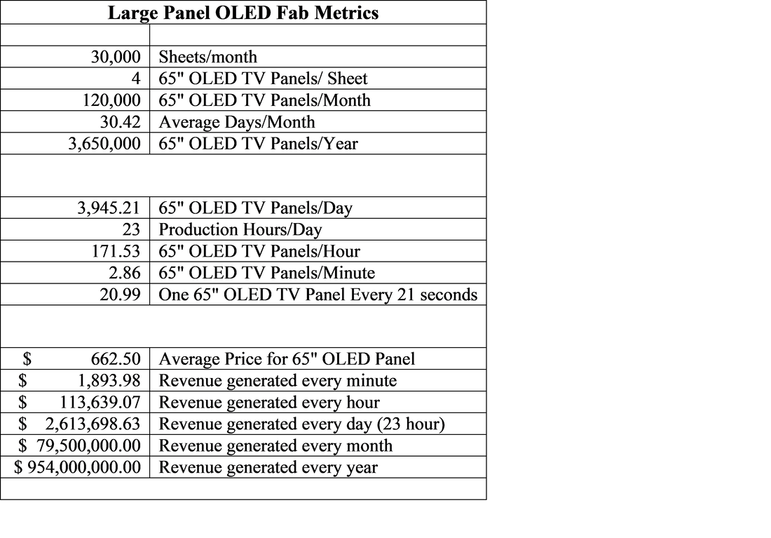
We note that these numbers represent a fab that has full utilization and 100% yield, which of course, is theoretical rather than practical, although that is the ultimate objective of every fab manager. A new OLED Gen 8.5 fab would likely start production at a low yield, which could be anywhere from 30% to 50% depending on the experience of the engineers, with relatively rapid yield improvements for experienced producers such as LG Display (LPL), but the sensitivity to yield at these unit volumes is quite large. A 1% improvement in yield amounts to a $795,000 gain over one month, so fab managers are extremely interested in yield improvement, especially in the early days of mass production at a new fab.
Panels are examined at a number of points during OLED panel production to reduce the number of defective panels that pass further down the process line, particularly the deposition stage where expensive emitter materials are added. Before deposition this is usually done through an optical process, but each fab is different in whether they use AOI (Automated Optical Inspection) tools that are in-line or tools that are off line. In-line tools must have TACT times that are compatible with production lines or multiple tools would be necessary to alleviate bottlenecks, or the fab can choose to ‘spot check’ by taking random panels off the line for inspection, a lower cost alternative but one that could miss less frequent defects.
The testing process becomes the most sensitive right before and right after the deposition of OLED materials, as pulling a defective substrate off the line before deposition is a major cost savings, and, albeit less so, poor deposition results would prevent the panel from incurring further cost, but the tests following deposition are more complex and require more sophisticated and expensive tools that deal with particular defects that are specific to OLED, some of which require a panel to be tested using a process that changes the characteristics of the OLED materials, which makes them unusable. Fab managers have to weigh the cost of pulling a set number of panels out of the line and destroying them to facing the chance that customers will be facing a defective panel that went undetected.
A research team at the Korea Institute of Science & Technology (KIST) have come up with a way to test OLED panels at an ‘intermediate’ stage, meaning after deposition but before encapsulation, that is not destructive. Testing OLED panels using a contact method is destructive but necessary, while testing them using a non-contact (UV irradiation) is also destructive, so the ‘cost’ of testing OLED TV panels is a yield reducer but carries significant financial risk if the defective panels reach consumers. The researchers at KIST have found a way to test for defects in OLED material deposition that uses terahertz waves that do not affect the materials themselves, particularly blue OLED emitters which age faster than other OLED materials, and is therefore non-destructive.
Terahertz waves, which are an order of magnitude higher than the gigahertz spectrum used for cell traffic, can penetrate the very thin layers of OLED materials, but are stopped by thick substances, and can be used to create high resolution images of the interior of thin films without their destruction. If the research is able to translate these results (Yeongkon Jeong, 2022) into a practical product, it would go a long way toward improving OLED panel quality without reducing yield, and while we don’t usually note such basic research, its non-destructive characteristics make it viable for examining thin films or ultra-small structures like Micro-LEDs and is therefore extremely relevant to the display industry, regardless of how it evolves over the next few years.
 RSS Feed