Fun with Data – Wafer Basics
Silicon wafers are the foundation of the semiconductor business, with the supply/demand balance a major factor in chip level pricing, although to the average investor a wafer is a wafer, but there is a bit more nuance that can give a bit more understanding of how the semiconductor industry functions, and “The intelligent investor is a realist…” (B. Graham).
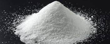
Silicon wafers are grown from metallurgical grade polysilicon, which is produced by mixing silica (Silicon Dioxide – SiO2) with Carbon and heating to 1,900⁰C in an arc furnace and is then converted to TCS (Trichlorosilane – SiHCl3), a liquid and further refined through distillation. The TCS is then converted to solid polysilicon through the Siemens process, and then reheated in a crucible (Czochralski Method). A seed crystal is dipped into the melt and is slowly pulled from the liquid as the silicon grows around the seed. By controlling the heat and ‘pull’ rate, the size of the silicon rod can be set.
Silicon wafers are grown from metallurgical grade polysilicon, which is produced by mixing silica (Silicon Dioxide – SiO2) with Carbon and heating to 1,900⁰C in an arc furnace and is then converted to TCS (Trichlorosilane – SiHCl3), a liquid and further refined through distillation. The TCS is then converted to solid polysilicon through the Siemens process, and then reheated in a crucible (Czochralski Method). A seed crystal is dipped into the melt and is slowly pulled from the liquid as the silicon grows around the seed. By controlling the heat and ‘pull’ rate, the size of the silicon rod can be set.

Basic Siemens Reactor - Source: https://ieeexplore.ieee.org/document/6178756
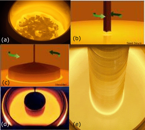
Czochralski crystal growth: (a) meltdown; (b) seed dip; (c) top; (d) shoulder; (e) body - Source:https://ieeexplore.ieee.org/document/6178756
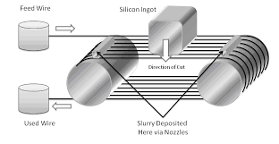
After the crystal cools it is ground down to more exact tolerances and the top and bottom are trimmed and eventually returned to a subsequent melt. The silicon ingot is then sliced into wafers with either a wire saw or a diamond blade, edges are defined, and the wafers are then ground or lapped to flatten the surface and then etched to remove any physical imperfections. The wafers are polished using a colloidal silica slurry that includes not only the physical surface polishing, but a chemical reaction that oxidizes the wafer surface. Then the wafers are cleaned using a number of chemicals, each to remove a specific type of contaminant. While this is a very simple explanation of the wafer process, it is a complex process and many steps are done in various level clean rooms, so understanding the intricacy of the process gives a better understanding of how the wafer market operates.
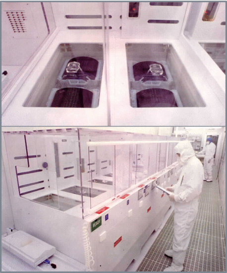
Wafer cleaning 'wet bench' - Source: ieee

BAsic Silicon Wafer Processing Steps - Source: ieee.org
On a general basis bigger is better with silicon wafers although production cost rise as they get larger, but at a lesser rate than the number of dies that can fit in the larger wafer[1]. That said, wafers are circular and die are usually square or rectangles so die that overlap the wafer edge must be compensated for by adding an edge exclusion metric and as die need space between them, room for ‘scribe lines’ and ‘singulation’ spacing must also be calculated so the die can be removed from the wafer individually. But there is also a very important factor that has a far greater effect on wafer production and that is the fact that there are only a few companies that dominate the silicon wafer business, and their ability to anticipate industry demand makes all other wafer calculations almost immaterial. But its Friday, the end of the summer, and the old clock on the wall says its time to take a walk outside before the leaves are off the trees, so we will continue with ‘Wafer Basics’ next week. Stay tuned.
 RSS Feed