Getting Smaller
5nm semiconductor process technology is at a premium and with only two foundries operating at that process level, others, or at least the few that could potentially afford the R&D and equipment cost of such a node are working toward similar production. That said, both Taiwan Semiconductor (TSM) and Samsung remain the only mass production fabs at 5nm. While semiconductor roadmaps allow for 4nm or potentially 3nm projects, IBM (IBM) has pushed the limits of Moore’s Law and announced it has developed the world’s first 2nm chip. Using current terms however to describe transistor dimensions is a bit wonky, as earlier generations considered the two dimensional size of transistors, while today’s terminology describes three dimensional components, which means a 2D comparison of actual transistor size would not show the expected size reduction as structure stacking (3D) adds to component counts and gives an ‘equivalent’ to what would be a 2nm chip.
That said, the transistor density is till the measurement point for process nodes, and while they vary from manufacturer t manufacturer and fab to fab, the table below gives an idea of the density of transistors from various manufacturers at each process node, shown as ‘millions of transistors/mm2, and how they can differ. IBM is using a 3 stack configuration to achieve higher densities (assumed) while Samsung will introduce a 3 stack cell at the 3nm node, while TSM is expected to wait until the 2nm node. While IBM uses Samsung’s foundry services for much of its actual chip production, it is likely a jump ball as to who will be first to use the technology, which based on the estimates, would see a performance increase of 45% and an energy consumption reduction of 75% relative to the 7nm process.
That said, the transistor density is till the measurement point for process nodes, and while they vary from manufacturer t manufacturer and fab to fab, the table below gives an idea of the density of transistors from various manufacturers at each process node, shown as ‘millions of transistors/mm2, and how they can differ. IBM is using a 3 stack configuration to achieve higher densities (assumed) while Samsung will introduce a 3 stack cell at the 3nm node, while TSM is expected to wait until the 2nm node. While IBM uses Samsung’s foundry services for much of its actual chip production, it is likely a jump ball as to who will be first to use the technology, which based on the estimates, would see a performance increase of 45% and an energy consumption reduction of 75% relative to the 7nm process.

While this sounds very significant for IBM to be the first to develop chips at 2nm, we say develop because IBM will not be a producer of such a device given they sold their manufacturing facilities to Global Foundries (pvt) 7 years ago, with the R&D work being done in their Albany, New York research facility. That said, they have partnership agreements with all three potential producers and we expect are in discussions as to how the technology implementation will progress, despite the necessity for mass production EUV and other process tools that need to be developed for such a device, so an actual 2nm processor is still a 2024 (or later) project.
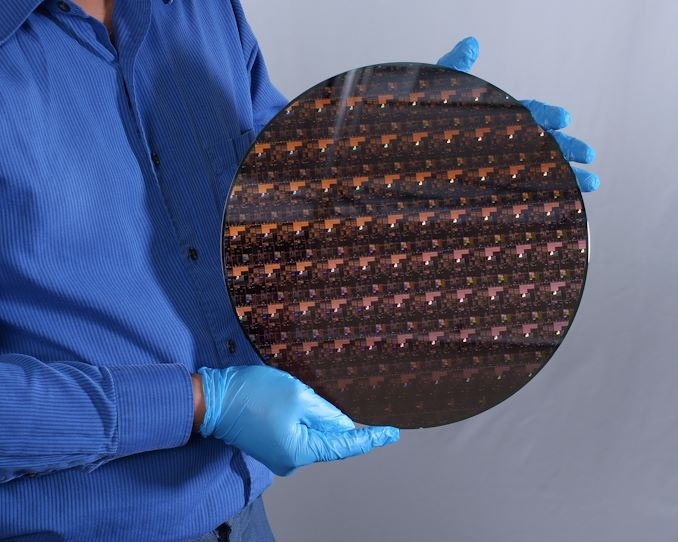
2nm process chips on 12" wafer - Source: IBM
 RSS Feed