HKC and Mikro Mesa to build Micro LED lab in China
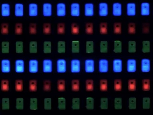
Taiwanese start-up Mikro Mesa (pvt) and HKC (248.HK) have agreed to collaborate on the development of micro-LED technology through a jointly funded development lab to be built in Chongqing, China. The lab, which is expected to be completed by the end of this year is expected to be producing micro-LED displays by 2018. Micro-LED technology is based on extremely small LEDs that can produce an emmissive display similar to OLED displays, but at lower cost (theoretically).
Mikro Mesa and others have been working toward reducing the size of such LEDs to match the resolution of both LCD and OLED displays, but have found issues such as light leakage (between LED pixels) and high power consumption and heat generation have increased the need for further development of the technology. By reducing the size of each LED, the power consumption and leakage can be reduced, and 50μm x 50μm LEDs can be potentially used for large displays that do not need the high resolution expected in TVs. Moving the technology to the consumer display space however, would entail reducing LED sizes, which is the direction of the joint development project.
Mikro Mesa has developed a 3μ x3μ LED that is said (by the company) to have no leakage, and will continue to be upgraded until potentially available to be used in consumer devices, and a variety of other companies are pursuing the same goals, with Apple having purchased LuxView in 2014, and development projects at both panel producers and LED chip suppliers. That said, the issues with micro-LED technology go a bit further, as the devices are so small that once manufactured, each LED has to be placed on a display substrate and connected, which is no easy task when working with chips in the 5μm size range at pixel densities of 40/inch for a 55” Full HD display or 80/inch for a 55” 4K TV display (+/-0.5μm placement tolerances are necessary). Manufacturing bottlenecks can make the large scale production of such displays problematical, and specialized methods of chip manufacturing and placement techniques are needed to make the technology competitive. Sony (SNE) has released LCD TV sets using micro-LEDs for backlights, rather than as the emitting source, but they remain LCD TVs with the same filters, polarizers, and other LCD components, and do not directly address individual pixels as does OLED technology.
Micro-LED Structure - Source: Technews.com
 RSS Feed