Micro-LED Basics – Part 1
Note: As Micro-LEDs get more press, we thought it helpful to help generate some basic understanding of what micro-LEDs are and how they are made. We will offer the series in relatively small chunks with the first below. Stay tuned for more…
Micro-LEDs are being touted as a potential game-changing display technology, but not unlike other revolutionary display technologies, micro-LEDs will not come easily. While they have some unique properties that make them well suited for displays, some of those same characteristics present potential problems that at best can take a significant time to conquer, and at worst, could keep the technology from ever being fully commercialized. That said, before we cast a negative pall over micro-LEDs, we also note that they have the potential to become a replacement display technology for almost any display application, once major stumbling blocks have been removed, so there is significant capital, time, and other resources being spent toward solving such problems, and similar challenges facing other display technologies were eventually addressed and met with solutions that enabled them to become major display technologies.
In order to understand the potential of micro-LED technology, it is essential to understand what they are and how they are produced, with the understanding that few of these processes, materials, and equipment, are in either a final stage of development or have even met some consensus in the industry as to how they will be used or implemented, making the micro-LED space a fluid one, and not surprisingly, one that can change daily, weekly, or monthly. There are some basics however that are.at least for now, inherent in understanding micro-LEDs, and we try to bring them to light below.
Micro-LED substrates
Micro-LEDs are similar to more typical LEDs used in LED lighting and as edge or direct-lit backlights used in LCD displays, however they are, as the name implies, considerably smaller. There is no ‘official’ size that would make an LED be called a micro-LED, but on a general basis, standard LEDs range from about 5mm, which is the size of this ❿, down to .5mm or 500um. Below 500um, such LEDs are called mini-LEDs, but once they go below 100um, they are generally called micro-LEDs. For reference, a 5mm LED chip is .196” across, meaning about 5 could fit in a 1” line (no spaces) and 25 in a 1” square. A 500um mini-LED is 0.019” inches wide, meaning 52 could fit in a 1” line, or 2,770 in a 1” square, and a 100um micro-LED is 0.039 inches across, with 254 in an inch and 64,516 in a 1” square. Micro-LED displays used for near-eye applications such as AR or VR, can be as small as 2um, which is .0000787” wide, with 12,700 in an inch and 161.29m in a 1” square.

Producing LEDs is usually done on a sapphire crystal substrates grown in a high temperature chamber using the Kyropoulos method, which uses high purity aluminum Oxide that is heated in a tungsten crucible with a ‘seed’ crystal on which the material ‘grows’ as the temperature is gradually decreased. The resulting 'boule' which can be as large as 300 kg, is them sliced into wafers and polished. While the sapphire crystal has a particular orientation, meaning the way in which the crystal structures are linked, the surface of the sapphire crystal must be free from imperfections, and given how small micro-LED are, even the smallest hairline crack or pit could ruin a large group of micro-LEDs. Each wafer is microscopically examined before it is used to verify its usability and in some cases a microscopic map is made of the surface.
There are other potential substrates for LEDs, with SiC (Silicon Carbide), Silicon (Si), and Gallium Nitride (GaN) being most researched, as each has advantages and disadvantages (cost is a big factor with silicon being the cheapest and GaN being the most expensive), but for the purpose of this note, we are focused primarily on sapphire substrates.
There are other potential substrates for LEDs, with SiC (Silicon Carbide), Silicon (Si), and Gallium Nitride (GaN) being most researched, as each has advantages and disadvantages (cost is a big factor with silicon being the cheapest and GaN being the most expensive), but for the purpose of this note, we are focused primarily on sapphire substrates.
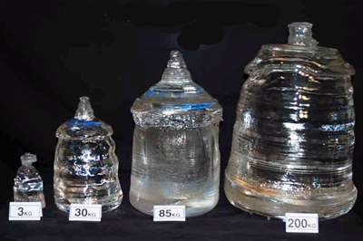
Sapphire Boules - Source: Rubicon
Again in a typical setting, the wafer is polished by the wafer producer or outside service and then shipped to the LED producer. The wafer is then examined again, cleaned, and loaded into a cassette that is used to automate the MOCVD (Metal Oxide Chemical Vapor Deposition) process. The cassettes are loaded into a handler that sits between two MOCVD tools and loads them into the deposition chamber of each tool, which could be set-up to take eight 6” inch wafers or five 8” wafers. We note that in terms of raw wafer surface area the 8 by 6” configuration is 20% larger which would imply higher throughput, but there are other considerations that also come into play in that decision, and there are also a number of single 8” wafer systems that clustered around a cassette handling system..
Once the wafer are placed in the MOCVD deposition chamber they are rotated individually at high speed (2,500 RPM) and depending on the particular MOCVD tool the entire susceptor plate (the metal wafer holder – Fig. 2) also spins. In some tools the materials to be deposited enter the chamber through what is called a showerhead that is close to the wafers, with the spin allowing the wafers to be covered uniformly. In other MOCVD tools the deposited materials are passed laterally across the spinning wafers in a configuration called ‘laminal flow’, which implies no turbulence in the materials, producing a uniform coating.
Once the wafer are placed in the MOCVD deposition chamber they are rotated individually at high speed (2,500 RPM) and depending on the particular MOCVD tool the entire susceptor plate (the metal wafer holder – Fig. 2) also spins. In some tools the materials to be deposited enter the chamber through what is called a showerhead that is close to the wafers, with the spin allowing the wafers to be covered uniformly. In other MOCVD tools the deposited materials are passed laterally across the spinning wafers in a configuration called ‘laminal flow’, which implies no turbulence in the materials, producing a uniform coating.

Susceptor Wafer Configuration - 8x6& 5x8 – Source: SCMR LLC
In the past the type of material flow corresponded to a particular manufacturer and was a selling point that meant choosing one tool vendor or another, but now Aixtron (ARXA.GR) produces tools in both configurations, which allows customers who prefer a particular configuration to vendor options. Veeco’s (VECO) MOCVD tools tend to be laminar flow oriented. As we have not seen any data that gives one configuration a distinct advantage over the other, it seems to be a personal preference of the customer, likely driven by what they already have. It’s not a hard and fast rule but parts and service costs are always lower if the tools are similar, so there is some stickiness to the choice of vendors. There is also the choice of the orientation of the reactor (horizontal or vertical), again a preference of the customer.
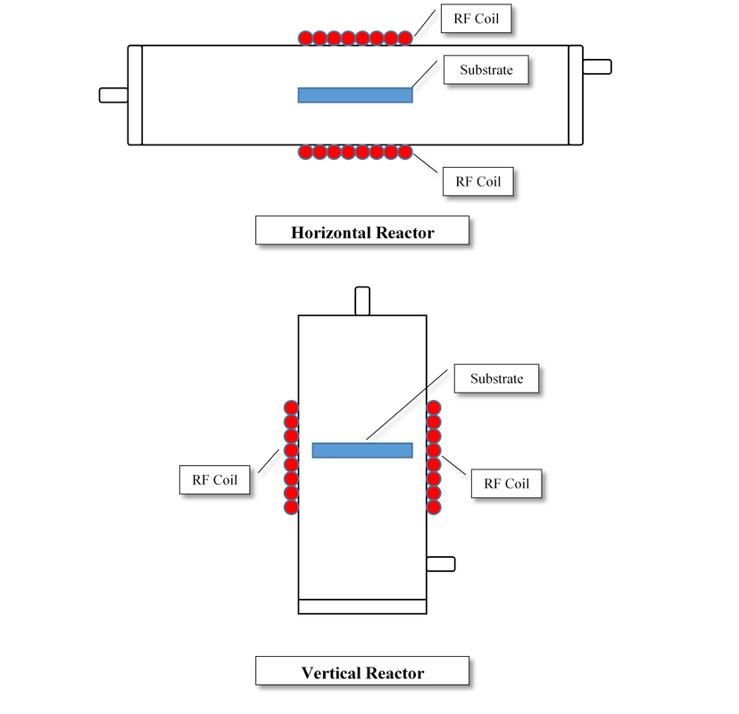
Horizontal/Vertical Reactor Configurations - Source: SCMR LLC
Materials are released into the reaction chamber with a carrier gas (usually Nitrogen , Argon, or Hydrogen) where the wafers are heated to between 500®C and 1500®C, with some reactors being hot-walled, meaning the walls of the chamber (usually graphite or quartz) pick up the heat in the reaction chamber, while others are cold-walled, where coolant keeps the reactor walls at a lower temperature than the wafer surface, which means it accumulates less reactant materials. For most LED type structures the materials that are sent into the reactor chamber are known as precursors, meaning they are not what is needed to create the final LED layers but are reactants that combine on the surface of the wafer to create the final structure.
Typical precursors are Trimethylgallium or TMG, TrimethylIndium (TMI), and Trimethylaluminum (TMA), which supply the heavy metals, Arsine (AsH3) and Ammonia (NH3). The materials react to each other on the surface of the wafer, hence the term Chemical Vapor Deposition and byproducts are pumped from the chamber. We note that these are volatile and dangerous materials and are extremely hazardous to the environment, so the cost of disposing of such materials and agents used to clean the chamber must be included in any cost of ownership calculation.
Typical precursors are Trimethylgallium or TMG, TrimethylIndium (TMI), and Trimethylaluminum (TMA), which supply the heavy metals, Arsine (AsH3) and Ammonia (NH3). The materials react to each other on the surface of the wafer, hence the term Chemical Vapor Deposition and byproducts are pumped from the chamber. We note that these are volatile and dangerous materials and are extremely hazardous to the environment, so the cost of disposing of such materials and agents used to clean the chamber must be included in any cost of ownership calculation.
Each layer of the materials needed to create the LED structure is deposited through similar chemical reactions until the entire wafer is coated with what amounts to a stack of materials. Once the deposition process is completed, the wafers are removed from the chamber and move to the etching process where resist, etch materials and masks are used to remove some of the layers to create individual LED structures.
More to come…
More to come…
 RSS Feed