Micro-LED Bottleneck Removers
In most of our notes on Micro-LEDs, we have focused on a particular aspect of the micro-LED process, that of transferring these extremely small LEDs from a die or carrier to a substrate, as the speed and accuracy of this part of the process is a large determinant in the overall cost of micro-LED systems. In those notes we discussed a number of ways in which moving such vast numbers of micro-LED die could be accomplished, from simplistic pick & place techniques to highly sophisticated laser-based systems. In those discussions, we noted that some systems were passive and some were active, while some required pre-processing and post-processing steps.
Passive systems transfer die. The transfer each die and have no way of knowing whether the die being transferred is good or bad. In such truly passive systems, the die that have been transferred have to be individually tested on the final substrate and any die that do not meet spec have to be removed and replaced. The time for the transfer, post-testing, individual die removal and replacement, and retesting, all contribute to the time it takes to produce a 100% fully functioning micro-LED display and obviously its cost. Transfer processes such as stamps and roll-to-roll are such passive processes, and while they are far less expensive tools than active systems, they reworking that they require must be added to the total system cost, with the reminder that a typical 4K micro-LED display would have 24,883,200 LEDs that are between 50um and 100um in size, which makes them about the same size as a human hair.
Active transfer systems are different in that they require a way to discover which die do not meet spec before they are transferred, eliminating the expensive and time consuming rework process. This is typically done in the semiconductor space with a probing tester that attaches to the leads of a chip or IC and tests for various electrical functions. This is not a problem when you are testing a relatively small number of complex semiconductor devices, but not effective when you need to test millions of relatively simple but very small LEDs. In order to create a KGD map (Known Good Die) LED tool vendors are adapting methodologies for testing such large numbers of LEDs using high resolution optical cameras, but even these, which typically focus on one die at a time, are to slow for such small die and such large numbers. Newer systems that can view much larger clusters of die are becoming available to speed up the process, but even these systems are only looking at the physical characteristics of the LED die, which can recognize physical issues but not specification faults such as luminance or color issues on individual or groups of die.
Newer systems have attempted to take die mapping even further, using lasers to ‘stimulate’ each die, which causes each die to radiate a heat pattern that can be mapped. While this does not give absolute specification data, it does show a completely different picture of the die, as shown in Fig. 1. This data is converted into a ‘map’ of the die, which many of the active transfer tools can use to skip the transfer process for those die that have been excluded from the KGD list, which avoids the post-transfer rework steps. Again, the time for creating the KGD map has to be added to the overall process time and cost of the micro-LED, and the fact that just ‘skipping’ the bad die during transfer can slow the process down must also be considered, but as these transfer tools continue to evolve, they reduce the cost of the process and bring the technology closer to becoming competitive with other display modalities.
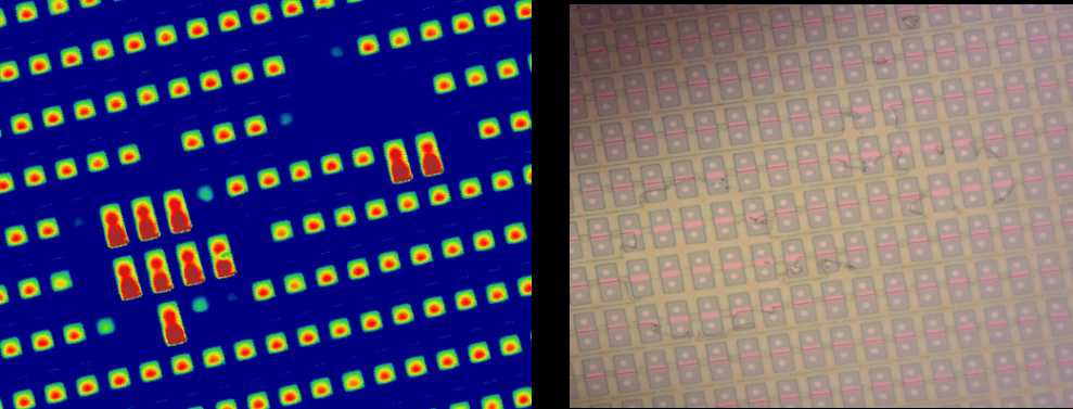
Comparison of Laser Stimulation and Optical Mapping - Source: Etamax
 RSS Feed