Supply Chain Market Research - SCMR LLC
  • Blog
  • Home
  • About us
  • Contact

May 12th, 2017

5/12/2017

0 Comments


The next Google Pixel phones
​

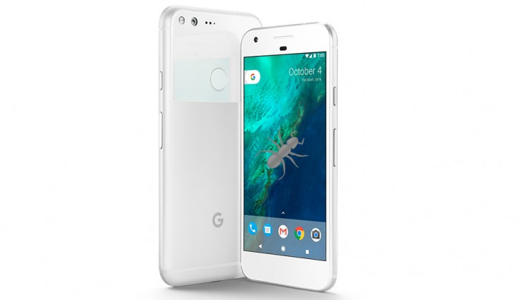
While not receiving the best reviews from a very jaded set of smartphone reviewers, the Google (GOOG) Pixel smartphone does not look like it is going to depart any time soon.  Google has been rumored to be developing two new Pixel2 models and now a potential third has surfaced.  Google released its Pixel and Pixel XL smartphones last October with 5” and 5.5” OLED screens at 441ppi and 534 ppi respectively using Qualcomm (QCOM) chipsets displays from LGD, and fairly standard features.  Google’s intent was to create a smartphone that could directly compete with the iPhone 7 (they both sell for the same price) with a focus on integration of all Google services, and while this is the 1st ‘Google branded’ offering from the company, the Nexus brand series of smartphones was also a Google offering.
The next generation of Google phones codenamed Muskie[1] and Walleye[2] are now expected to be joined by Taimen[3] (What’s the deal with fish names?), a 3rd variant that is expected to have a larger OLED screen than the other two models.  Google has been planning to invest $900m with LG Display to gain access to LGD’s flexible display capacity but will likely be unable to meet volume expectations this year.  We understand Google’s desire to create a smartphone that will give its vast user base access to the world of Google through a mobile device, but at what cost?  The smartphone market, even for the most experienced and well-known brands, is a minefield that seems to get more treacherous each month, and Google has not knocked the cover off the ball with its previous mobile offerings.  LGD is happy, with another customer to justify its small panel OLED business, but without something new, the Google brand seems a ‘me-too’ entry.  The company does have the ability to create applications that are eminently consumer centric, and given the AI orientation of the consumer electronics space, this could give them an edge, but it remains difficult for smartphone companies to become leaders without something that is ‘shiny and cool’, despite the helpful applications.  Maybe the Taimen model will do the trick, but it will be competing with a new iPhone and a stack of other smartphone offerings that will be available later this year or early next.  Push the envelope Google…and lay off the fish names.


[1] Short for Muskellunge – a large fish in the Pike family

[2] Another smaller fish in the Pike family

[3] A large fish in the Salmon family
Picture
Taimen Google Smartphone - Source: Geekbench
0 Comments

May 12th, 2017

5/12/2017

0 Comments


Samsung Display denies construction of new OLED fab

Last month (4/24/17) we noted that Korea based UBI Research had indicated that Samsung Display (pvt) has begun construction of a new Gen 7 flexible OLED fab in Asan, South Korea.  The original story from Maeli Business News was likely stimulated by the fact that Samsung Display has been leveling the land adjacent to its existing manufacturing site in Asan, but the company has now said that it has not decided what it will do with the additional property.  The speculation surrounding the ‘potential’ new fab, designated A4 (A1,A2, and A3 are Samsung’s main OLED display facilities) was that it would be a Gen 7 line with a maximum capacity of 135,000 sheets/month, with an opening date of sometime in late 2018.
As we noted previously, we have not included such a fab in our OLED industry model, as we need confirmation from at least two sources to make such an inclusion.  That said, we note that if the fab were built to those specifications and fully built out, it would add (by 4Q 2018) 17.8% to Samsung Display’s OLED capacity, not an insignificant amount.  Given that we believe the small panel OLED space will remain capacity constrained for a number of years, the idea that Samsung Display would want to build out as much capacity as possible is not a strange one, but at the same time Samsung Display management has to evaluate the impact of new fab construction, low initial yields, and changing demand, before adding a new fab to its OLED construction schedule. 
Filing the story under “The lady doth protest too much, methinks”, we expect Samsung Display has an idea for the land in mind, but is not ready to reveal such plans to the public.  We could speculate that they are negotiating with Apple (APPL) for a dedicated OLED fab, or are thinking of establishing an OLED line that uses non-traditional deposition techniques, but with Apple a new entrant into the OLED space and other smartphone brands in the early stages of OLED adoption, it would seem a high risk venture, even for Samsung Display, at this time.  We note our Samsung Display quarterly smartphone unit volume estimates[1] in Fig. 1, which do not include the A4 fab.


[1] Details of assumptions available on request
Picture
Samsung Display Quarterly OLED Smartphone Unit Volume Estimates - Source: SCMR LLC
0 Comments

May 11th, 2017

5/11/2017

0 Comments


Chinese LCD material company to enter OLED materials market

Zhejiang Yongtai Technology Co. (002326.CH) has completed a feasibility study concerning its entry into the OLED materials market.  The company, which provides liquid crystal to the display industry, along with pharmaceutical and agricultural chemicals, will invest $13.76m US of its own funds to build out OLED material production capacity with a goal of 60 tons/year.  According to recent studies, the value of organic materials in OLED products is ~8%[1] which would imply an organic materials market of $1b of which intermediate chemicals would represent ~15% or $150m US, but we note that what is included or excluded from these statistics can be quite significant as to stated market sizes.
The company has indicated that it believes China accounts for much of the worldwide OLED intermediate material market share and can become a significant refiner of intermediate OLED materials due to lower cost and process advantages.  Further, they believe that domestic OLED display producers will favor local OLED material producers, as long as quality is maintained.  The project is expected to take 1 year to construct, with an expected output of ~30%, with 100% reached in the following year.  The company also expects to see an annual net profit of $6.68m/year with an annual ROR (after tax) of 56.8% and a 3.6 year after tax payback period.
While we are unsure of the actual OLED materials that will be produced at the new facility, the company’s goals are aggressive, particularly from the perspective of OLED materials.  The production of phosphorescent OLED emitters, which would have the highest value/gram of materials in a typical OLED stack, would be limited by worldwide IP, which is held by Universal Display.  That would leave lesser OLED stack materials, which have both a lower price/gram and face much greater competition from other specialty chemical companies.  China does need to build out its OLED material supply chain, but the most important characteristic of OLED materials is their purity, as even miniscule impurities can cause significant problems.  If Chinese companies are able to produce end-user ready OLED stack materials that meet current standards, they will become eminently successful, even if their pricing is the same as what is currently available, however thus far we have seen little indication that such is the case, with OLED panel producers in China focused on the same OLED material suppliers that are used by Samsung Display and LG Display (LPL), the share leaders in OLED display production.


[1] Displaysearch 2015
0 Comments

May 11th, 2017

5/11/2017

0 Comments


Is China Star to become a listed company?

TCL (000100.CH), the parent of China Star (pvt), the 2nd largest display producer in China, is undergoing a reorganization, and while the reorganization is intended to integrate the display producing organizations owned by TCL into a more integrated unit, there is considerable speculation that the reorganization would also include the listing of Huaxing Photoelectric, also known as China Star.  Currently shares of TCL are suspended from trading on the Shenzhen exchange until May 21, as is customary during reorganizations for Chinese companies.
A listing for China Star would help to isolate the display production portion of TCL from its other businesses, which include TCL Multimedia Technology (01070.HK) which is among the largest TV manufacturers and distributors in China and worldwide, TCL Communications Technology (02618.HK) which produces mobile devices under the TCL and Alcatel brands, Tonly Electronics (01249.HK) an ODM for audio and video products and TCL Display Technology (00334.HK), which includes China Star Optoelectronics.  TCL is also a major appliance brand in both China and in Asia, although Chinese competitor Haier Group () is the largest in both China and the world, followed by US based Whirlpool ().
As a display producer, China Star has 4 production facilities in Shenzhen and Wuhan, ranging from Gen 4.5 to Gen 8.5 and is building a Gen 11 ultra-large panel fab which is expected to begin phase 1 production in 2Q 2019, with some capacity for large panel OLED TVs (unconfirmed).  When completed, this fab will have the largest substrate format of any display production fab at 11.52 m2/sheet (124 ft2), with Asahi Glass (5201.JP) being the co-located substrate supplier.  China Star also runs a Gen 4.5 OLED pilot line and is building a Gen 6 OLED production fab based on LTPS backplane technology, which will likely be for small panel OLED production.  That fab is expected to open in 3Q 2018.  On an overall basis, we believe China Star has a 6.4% share of worldwide display capacity this year (up from 5.2% last year) and will reach 7.2% by 2020.
Picture
China Star Gross Capacity - 2011 - 2020 - Source: SCMR LLC, Company Data
Picture
Chinese Panel Producers - Market Share - 2004 - 2020 - Source: SCMR LLC, Displaysearch, Company Data
0 Comments

May 11th, 2017

5/11/2017

0 Comments


UBI Predicts substantial Light Emitting Materials market growth

Korean based UBI Research is predicting substantial growth in the light emitting materials market between 2017 and 2021.  According to their estimates, the overall light emitting materials market, which in this case relates to materials used in OLED displays, is expected to grow from $957m this year to $3.36b in 2021.  Figure 1 illustrates the UBI data, along with Rate of Change data for the LE materials market, and overlays for raw and available OLED capacity rate of change.  The rate of change data gives some indication as to the match-up between LE material market growth and industry capacity growth.
We note that UBI predicts that the ASP of light emitting materials will drop by 5% to 10%/year and that there is a 5% to 30% recycle ratio on LE materials, however we are not as sanguine as they are on both the price decline and the recycle ratio.  As Universal Display (OLED) is the largest supplier of OLED materials, and they have an emitting material discount program that is based on volume, we believe that the ASP on some materials will decline faster than the 5% to 10% that UBI predicts.  Green emitting material, which is part of an RGB OLED stack in many small to medium sized OLED displays, is used in a higher proportion than red emitter material, and consequently travels down the volume discount timeline faster than red material.  To UDC’s credit, new light emitting materials, when adopted by OLED producers, reset the discount timeline back to starting ASP levels, such as what happened with the adoption of a new red emitter material for the Galaxy S8, but such changes do not happen quickly, and as capacity at dominant producers increases, so will the speed at which volume discount points are reached.
Another factor that was not mentioned by UBI, that we consider in our OLED industry and company models, is efficiency.  In typical OLED evaporative processes, much of the emitter material is wasted, either on the metal mask used for patterning, or on the walls of the evaporation chamber itself.  Efficiencies of 25% or 30% were not uncommon for older deposition equipment, although newer tools can see production efficiencies to 60%, but a primary focus of OLED panel producers is to both increase overall yield and reduce cost, with the latter being focused on reducing material waste.  As new deposition equipment is designed and implemented, material usage efficiencies will continue to increase and will offset some of the industry capacity growth, but the real increment would come from a singular change in the OLED production process itself, by changing from evaporative deposition to a roll-to-roll process or an ink-jet printing process.  These alternative methods are being researched and tested by Samsung Display (pvt) and others, and have efficiencies in the 90% range.  While the light emitting materials used in these methods will be somewhat different than those used by current evaporative processes, it would be difficult for OLED material suppliers to offset the higher efficiencies with substantially higher ASPs.  While putting these processes in high-volume situations has not yet happened, we expect that by 2021 a portion of the light emitting materials market will be focused on materials for these high efficiency processes, which gives us a bit of caution in predicting LE material dollar growth in the out years.
We also believe that UBI is optimistic about the light emitting materials recovery rate.  While lower efficiency deposition tools should be ripe for material recovery, we believe that the purity of the materials needed for OLED deposition is so high that the cost of refining emitter materials is too high to make it worthwhile currently, and the use of higher efficiency processes will reduce the amount of recoverable materials substantially.  We do expect some of the less expensive materials are recoverable, but separating out the high cost emitter materials from a lower cost host and refining it back to original specs does not seem to be a cost effective way to reduce costs currently.  We do believe the light emitting materials market is poised for substantial growth over the next few years, but our optimism is tempered somewhat by the prospects for higher efficiency toolsets and volume based material pricing.
Picture
Light Emitting Materials Market & ROC - Source: UBI Research, SCMR LLC
Picture
Bosch-Rexworth Roll-to-Roll Production Tool - Source: Lucept
Picture
Kateeva Large Scale OLED Material Ink-jet Printer - Source: Kateeva
0 Comments

May 10th, 2017

5/10/2017

0 Comments


Black Cattle digs deep

Back in September of last year we noted that Chinese soybean and cereal producer Black Cattle Food Co (002387.CH) had decided to branch out and become a producer of OLED displays and we followed up with notes in October, November and a contract for OLED processing tools in January of this year.  While we had our doubts as to the viability of an OLED fab being built by a food processing company, we have to admit that things seem to be progressing.  The fab, which is being built in cooperation with Kunshan based Visionox (pvt), seems to have gotten off the ground, or at least in the ground.
We have information that the main pilings for the fab building will be completed by the end of this month, which means at least a portion of the funding for the Gen 6 OLED plant has been completed.  The original plan was for a total cost of $4.48b for the fab, with Black Cattle partnering with the Kunshan State Investment Group (34.28%), the Kunshan Yangchen Wei Business Group (12.28%) and Kunshan Venture Holdings (3.14%), although we do not know the state of the investment funding at this point.  We have to admit that we had very low expectations for this fab to even make it past the planning stage, but it seems that we were wrong and the fab is at least being built.  Our biggest concern is not the construction of the fab itself, but the concept that when fabs are being built by companies that have no direct contact with the industry, it has the potential to signal a top.  Wait, we do expect a slew of new OLED fabs to be built over the next two or three years, but every time we hear of a partially funded OLED fab being planned by a company with no stake in the industry our ‘dadar’ (display radar) blips, our ‘dpar’ (display paranoia) kicks in, and our Fennec-like ears perk up…
Picture
Fennec - Source: Viralnova.com
0 Comments

May 10th, 2017

5/10/2017

0 Comments


Samsung on Fire – Not in a good way

According to the Korean press, there was a fire at a Samsung Display fab in Cheonan yesterday.  The fire was reported at 9:20 AM and was extinguished by the local fire authority by 10:15 AM.  The fire, which started in a cooling tower on top of the 3 story facility, was part of the power and chemical supply system for the fab.  No casualties were reported and the company has not stated what caused the fire.  While we expect little impact to Samsung Display’s production goals, fires or other catastrophic events cause automatic shutdowns at display fabs, and evaluation teams must look at the fab structure and equipment to make sure there was no damage.  If the evaluation proves positive, we would expect the fab to be back in production within 24 to 48 hours.
0 Comments

May 10th, 2017

5/10/2017

0 Comments


Japan Display Reports 4Q and 2016 results

While Japan Display (6740.JP) updated expectations for 2016 results on May 1, they reported full results last night.  4Q sales results were 4.4% above forecast and up 36% y/y, but we note that results from all panel producers in the 1st half of 2016 were dismal as panel prices were in steep decline.  4Q operating income was below expectations, as was net income and forex loss, as the value of the yen was 3.3% higher than expectations, was 3.6b¥ ($31.6m US).  For the full year 2016 (ended March 31) sales were down 10.6% y/y with operating income up 10.7%, due to the easy y/y comparisons, but pre-tax, while better than last year, was still a ¥11.2b loss (-$98.4m US).  Mobile device sales represented 82.4% of 2016 sales vs. 84.7% last year, and automotive/consumer was 17.6% vs. 15.3% last year, with strong automotive results in the US and Europe offset by weaker consumer product results.
Japan Display indicated that 1Q sales are expected to be down 25% q/q but up 3.2% y/y, and operating income is expected to be ¥-15b, substantially below the 4th quarter’s ¥8b (positive) and last year’s ¥-3.4b.  The company cited seasonality, customer inventory, and new model launches as the reason for the 1Q sales drop, and higher fixed costs for the Hakusan fab and OLED R&D, as the reason for the operating loss.  On a general basis, the company also indicated that seasonality and product changeovers would weaken 2nd quarter Chinese sales.
For the full year 2017 the company plans to accelerate its OLED development, with a focus on flexible displays produced on its Ishikawa G4.5 LTPS OLED pilot line and is preparing an OLED pilot line on their Gen 6 line in Mobara.  They expect to begin pilot production this summer and full manufacturing in 1H 2018, which could be anywhere between April to September.  Our model calls for phase 1 capacity of 5,000 sheets in April 2018 and phase 2 capacity of 10,000 sheets in March 2019.  The company indicated that their OLED process was a real RGB stripe display, versus other OLED displays which shared a red or blue sub-pixel with a green one.
Picture
Japan Display OLED stripe configuration vs. typical Pentile configuration - Source: Japan Display
On a general basis, JDI continues to mandate a push to lower its break-even point and has implemented structural reforms by partially shutting down and consolidating assembly operations in China, but the company’s reliance on the mobile device business (aka smartphones) is still a significant issue, despite the effort to expand the automotive sales segment.  The company issued ¥45b ($395m US) of converts to the Innovation Network Corporation of Japan, a quasi-government organization that was responsible for the formation of Japan Display itself, and received a ¥30b ($263m US) loan from INCJ, with the converts used to fund R&D for printed OLEDs and the loan for R&D in OLED evaporative projects.  We note that the company shares in losses generated by JOLED (pvt), its soon-to-be OLED-only subsidiary. 
Needless to say, Japan Display has a significant incentive to speed up its OLED development as Apple (AAPL), JDI’s largest customer, is considering moving part of its iPhone production to OLED displays.  This represents a significant change for JDI and while they understand that should this happen, they will lose a portion of the Apple business to South Korean rival Samsung Display (pvt), they need to protect themselves by developing an OLED alternative as quickly as possible.  They do have both their own OLED assets and R&D and now have the same from OLED specialist JOLED,  but R&D and mass production can be very different animals and JDI needs to do this rapid OLED development while maintaining a viable LCD business, which we believe will be difficult at best.  We note that the acquisition of JDI’s controlling interest in JOLED, which was originally scheduled for the 1st half of fiscal 2017 has been delayed until the end of December 2017.
0 Comments

May 10th, 2017

5/10/2017

0 Comments


Samsung tries to up the game in low-end smartphones

While Samsung Electronics (005930.KS) is well-known for its flagship Galaxy S series in the US, the company has a number of other smartphone lines that are especially designed for other markets.  These phones, particularly those sold in China, tend to be mid-priced to low-end, as opposed to the high-end feature set and pricing of the Galaxy and Note lines.  China abounds with smartphone manufacturers that offer customers a subset of high-end features at considerably lower prices, with Xiaomi (pvt), originally starting the trend, and now followed by Oppo (pvt) and Vivo (pvt) among others.  In order to maintain share in these markets, Samsung Electronics had to develop specialized product (J, A and C lines) that could compete with those Chinese buyers who were interested in a smartphone, but were not interested in paying for a full featured Galaxy model.
Samsung remained iffy about some of its previous models, with limited availability of the ‘Pro’ models of these phones, and looked like they were just interested in holding share with ‘me too’ products that offset the slew of new Chinese models that continue to squeeze ASPs.  That said, we hear that Samsung is working on the next generation ‘C10’ smartphone and is looking to up their game a bit.  Expectations for the C10 are for a dual camera, which has propelled the few Chinese brands (Huawei (pvt), Vivo, iPhone 7+) that include such a feature into the top share categories, and while the actual specs of the C10 series have not been released, we hear fingerprint scanner, Bixby, Qualcomm (QCOM) Snapdragon 660 processor, and bigger battery are being considered to try to beat what is already in the field from competitors. 
The real question will be pricing, and availability, as the C9 Pro was in short supply in the Chinese market, but we doubt Samsung will price ay lower than other premium brands.  In such a case, the C series phone will have to be loaded with enough features that it can outperform almost all of its competitors.  Not an easy task on a limited budget, especially since the S8 relies on high cost components that Samsung uses to make sure it does not have another product meltdown like the Note 7.  We would expect a new C line product by October of this year.
Picture
'Leaked' Samsung Galaxy G10 - Source: BusinessKorea.com
0 Comments

May 09th, 2017

5/9/2017

0 Comments


Using OLEDs in an interesting way

Dresden based Fraunhofer FEP (pvt) has developed a unique application for OLED microdisplays.  The company has adapted an OLED microdisplay, built on a silicon substrate, to read fingerprints without additional optics.  The sensor both emits light that reflects off of the finger, and detects that light allowing for analysis.  The resolution of the sensor is 1600 dpi, which is 3x the required FBI resolution, and allows for the identification of very small sweat holes (What does your sweat hole pattern look like?) for more detail than is currently available.
The company expects the system to be adopted for mobile devices as the additional resolution will make it less susceptible to ‘spoofing’, and will be shown at the upcoming 2017 SID Display Week conference.  Just remember they can still cut your finger off and use it to gain access to your secret lair, unless your sweat holes have dried up and closed after digit removal….
Picture
Hi Res OLED on Silicon Fingerprint sensor - Source: Fraunhofer FEP
0 Comments
<<Previous
Forward>>

    Author

    We publish daily notes to clients.  We archive selected notes here, please contact us at: ​[email protected] for detail or subscription information.

    Archives

    May 2025
    April 2025
    March 2025
    February 2025
    January 2025
    January 2024
    November 2023
    October 2023
    September 2023
    August 2023
    June 2023
    May 2023
    February 2023
    January 2023
    December 2022
    November 2022
    October 2022
    September 2022
    August 2022
    July 2022
    June 2022
    May 2022
    April 2022
    March 2022
    February 2022
    January 2022
    December 2021
    November 2021
    October 2021
    September 2021
    August 2021
    July 2021
    June 2021
    May 2021
    April 2021
    March 2021
    February 2021
    January 2021
    December 2020
    October 2020
    July 2020
    May 2020
    November 2019
    April 2019
    January 2019
    January 2018
    August 2017
    July 2017
    June 2017
    May 2017
    April 2017
    March 2017
    February 2017
    January 2017
    November 2016
    October 2016
    September 2016

    Categories

    All
    5G
    8K
    Aapl
    AI
    AMZN
    AR
    ASML
    Audio
    AUO
    Autonomous Engineering
    Bixby
    Boe
    China Consumer Electronics
    China - Consumer Electronics
    Chinastar
    Chromebooks
    Components
    Connected Home
    Consumer Electronics General
    Consumer Electronics - General
    Corning
    COVID
    Crypto
    Deepfake
    Deepseek
    Display Panels
    DLB
    E-Ink
    E Paper
    E-paper
    Facebook
    Facial Recognition
    Foldables
    Foxconn
    Free Space Optical Communication
    Global Foundries
    GOOG
    Hacking
    Hannstar
    Headphones
    Hisense
    HKC
    Huawei
    Idemitsu Kosan
    Igzo
    Ink Jet Printing
    Innolux
    Japan Display
    JOLED
    LEDs
    Lg Display
    Lg Electronics
    LG Innotek
    LIDAR
    Matter
    Mediatek
    Meta
    Metaverse
    Micro LED
    Micro-LED
    Micro-OLED
    Mini LED
    Misc.
    MmWave
    Monitors
    Nanosys
    NFT
    Notebooks
    Oled
    OpenAI
    QCOM
    QD/OLED
    Quantum Dots
    RFID
    Robotics
    Royole
    Samsung
    Samsung Display
    Samsung Electronics
    Sanan
    Semiconductors
    Sensors
    Sharp
    Shipping
    Smartphones
    Smart Stuff
    SNE
    Software
    Tariffs
    TCL
    Thaad
    Tianma
    TikTok
    TSM
    TV
    Universal Display
    Visionox
    VR
    Wearables
    Xiaomi

    RSS Feed

Site powered by Weebly. Managed by Bluehost