Supply Chain Market Research - SCMR LLC
  • Blog
  • Home
  • About us
  • Contact

Sidestepping

5/17/2022

0 Comments


Sidestepping
​

​Chinese panel producers are masters of hyperbole, using words like ‘glorious’ and ‘world-changing’ to describe their successes, regardless of how they relate to the global display space.  That said, it can be difficult to get a direct answer from the same companies when things are not going in the correct direction, as was the case during an investor meeting with China’s leading LCD and OLED producer BOE (200725.CH).  After the company described its 2021 and 1Q 2022 impressive results in detail, management seemed to be less willing to give details when asked a few harder questions.
There was little detail given on how the company is changing its LCD production to maintain ‘good profitability’ during a difficult pricing period, other than saying the company’s performance is better than that of the industry and that such changes (whatever they are) are ‘a test process of the company’s products’, which we assume to mean that if the products are good, they will continue to sell regardless of the environment.  They did cite flexible OLED as the current growth driver and maintained their target of 100m flexible OLED units by the end of the year, up from a bit under 60m last year, also mentioning the depreciation that they will continue to ‘digest’ to improve performance this year.
When questioned about their expectations for panel prices, they stated that they did not expect a sharp decline in the future and mentioned a chance for a structural rebound as demand improved in 2H, but when asked specifically about the company’s utilization rate they stated that “Under different statistical calibers, the value of the utilization rate will show different values…The adjustment of the structure will lead to the change of the production line, but it does not necessarily mean that the utilization rate will change.  At present, the production line utilization rate of the companyis maintained at a reasonable rate,” which is about as close to a non-answer as possible.  The company also refrained from answering earlier investor questions about rumors that Apple (AAPL) has suspended accepting displays from the company recently due to undisclosed changes in panel structure made by BOE, but were happy to disclose that they were supplying panels for Hisense’s (600060.CH) line of Mini-LED QD TVs.
All in, despite the detailed questions, little real information was gained at the investor meeting and while the Chinese stock market gives both institutional and individual investors a platform for asking questions directly to management, it is rare that Chinese display companies reveal any information, especially when things are difficult.  Perhaps it might be a bit easier to read the true meaning of some of those statements if we were face-to-face but after years of hearing company-speak from US and other foreign companies, we expect the nuance would reveal little that was not already implied.
 
0 Comments

Quick Take – Taiwan Supply Chain

5/16/2022

0 Comments


Quick Take – Taiwan Supply Chain
​

​While we highlighted April results for Taiwan’s display producers last week, which were decidedly poor, we take a quick look at some of those in the Taiwan display supply chain to see how the Chinese lockdowns have affected April results.  Not all suppliers in the list below saw reduced April sales in keeping with the poor results see by display suppliers, as polarizer suppliers BenQ 8215.TT) and ChengMei (4960.TT) are booked through the end of June, although BenQ indicated that it is wary of 3Q prospects as price competition has increased considerably in recent weeks.  In most cases the reasoning given for the drop in April sales were the lockdowns in China, which limited availability of components and complicated logistics. 
The general feeling (our read) is that in the best case scenario is for a somewhat better 3Q as inventory levels are brought down this month and next, and while the build for the holiday season will be lower than originally expected, it will begin in July and help boost m/m sales results.  That said, it seems that those suppliers that were able to secure longer-term contracts and held higher component inventory levels have been able to sustain results through April, but will face weak y/y results in 3Q if the lockdowns continue.  We expect while China will continue to publicize its ‘No-COVID’ lockdown policy it will ease up on transportation restrictions for key industries going forward.   Lockdowns are certainly beneficial toward keeping COVID from becoming a country-wide epidemic in China but they also limit growth, especially in the areas where China is trying to maintain a competitive edge over Vietnam, Indonesia, and India..
Radiant Opto (6176.TT) – Backlight Supplier – Sales ↓51.3% m/m, ↓43.3% y/y
Global Lighting Technologies (4935.TT) – Display Light guide supplier – Sales ↓54.7% m/m, ↓55.1% y/y
BenQ Materials – Polarizer supplier – Sales ↑1.3% m/m, ↑3.6% y/y
ChengMei Materials – polarizer supplier – Sales ↑15.1% m/m, ↑21.7% y/y
Lite-On Opto (2301.TT) – LED supplier – Sales ↓9% m/m, ↑1% y/y
0 Comments

Samsung Orders Components for Foldables

5/16/2022

0 Comments


Samsung Orders Components for Foldables
​

​Samsung Display is said to have begun placing orders for the components needed to produce its next line of foldable smartphones and has increased the unit volume expectations considerably over last year.  SDC will begin display production in June and will begin assembly in July, likely at its expanded facility in Vietnam, which has increased capacity by ~33%.  The initial component unit volume is expected to be be for between 15m and 18m units, doubling the 7m units the company produced last year, with ~70% for the Galaxy Z Flip and 30% for the Galaxy Z Fold.
Without reviewing the vast number of ‘leaks’, ‘influencer rants’, and idle speculation about what the new foldables will look like or contain hardware-wise, we expect relatively little change over last year’s models with the exception of the inclusion of a holder for the S-Pen on the Z Fold 4.  Display sizes should be almost if not exactly the same, with the possibility of some camera improvements and battery size changes, but most important will be the price, as last year Samsung was able to bring down the initial price of the Z Fold by $200. 
There has been some conjecture as to the lower profitability of the foldable line for Samsung, which is logical considering the maturity of Samsung’s flexible OLED production experience relative to its foldable production experience (although still the leader in foldable OLED), but we expect Samsung has been working toward bringing down the price for the Fold/Flip 4 line, even in an inflationary market in order to stimulate sales.  Perhaps a $200 price reduction (bringing the initial price of the Fold 4 to $1,600 from $1,800 last year) is a bit much to hope for but at least Samsung has the volumes needed to squeeze a bit more out of its foldable supply chain.
The last two foldable model years have seen announcements of the new line made in early to mid-August, which we expect will be the same this year, with release dates by the end of August or early September depending on transportation issues, but we expect this will be a more competitive year for foldables, despite Samsung’s considerable lead in the space, especially in China where Vivo (pvt) and Honor (pvt) have joined Huawei (pvt) and Oppo (pvt) with offerings this year.  There is also considerable buzz that Samsung will release a rollable smartphone device this year although we keep our expectations low for such a model this year.
0 Comments

Japan Display Goes Litho…

5/16/2022

0 Comments


Japan Display Goes Litho…
​

Photolithography is the platform on which the semiconductor industry is built.  The concept of photolithography etch is fundamental to almost all semiconductor production and is the most common way in which structures at the micron level are formed.  In the display space however, photolithography is used in the formation of the TFT (thin-film) electronics that control display pixels, but the pixels themselves, at least in OLED displays, are formed using the deposition of OLED materials through CVD (Chemical Vapor Deposition) tools that vaporize the OLED materials and deposit them through fine metal masks, essentially screens that form red, green, and blue sub-pixels that generate the millions of color combinations needed for full color displays. 
There are problems with OLED material deposition, one of which is the masks themselves.  They are made of INVAR, a nickel-iron alloy that is able to maintain shape and uniformity under the temperature conditions used in CVD (up to 500⁰C) but at the same time must be unusually thin and placed extremely close to the substrate to create precise sub-pixel placement.  The requisite thinness limits the size of these masks, as they begin to sag above Gen 6 substrate size, and the buildup of material on the mask surface requires they be cleaned and replaced regularly, pushing OLED display producers to look for alternative deposition methods.
One promising technique is ink-jet printing where multiple nozzles place OLED material droplets on the substrate as they move across its length.  This allows for precise control over the materials, resulting in a substantial reduction in the amount of OLED emitter material waste but in order for the material to pass through the nozzles, it must be put into solution which means mixing the emitter materials with a solvent which can change the characteristics of the OLED materials or require ‘soluble’ materials that are different from those used in CVD deposition.
Picture
Fine Metal Mask - Distance distortion - Source: Decker, Wolfgang & Belan, Rob & Heydemann, Volker & Armstrong, Sean & Fisher, Tim. (2016). Novel Low Pressure Sputtering Source and Improved Vacuum Deposition of Small Patterned Features Using Precision
AR/VR displays require very high resolution displays in order to keep the optic system from becoming confused about what it is seeing (similar to motion sickness) and such displays require pixel densities far above the 400 to 500 pixels/inch we see in current smartphones, but both CVD deposition and ink-jet printing fall short of these densities, pushing OLED display producers to look for other alternatives to boost their ability to  create high density pixel displays and that is where the aforementioned photolithography comes in.  Japan Display (6740.JP) has announced that it will be starting to sample displays to customers this year that are based on ‘maskless’ lithography based material patterning.
JDI’s eLEAP (environmental positive Lithography with maskless deposition Extreme long life, low power, and high luminance Any shape Patterning) is claimed to increase emission efficiency by 60%, which is more than 2 times that of the FMM method and is not limited to Gen 6 substrates.  The process is green in that it is more ‘environmentally positive’ without masks that need to be regularly cleaned and therefore uses less toxic material and produces less CO2 emissions.  JDI is combining this technology with its expertise in IGZO TFT backplanes to create what it calls a breakthrough in display technology.
While we cannot verify many of JDI’s claims, there are some points that are do make sense.  We expect that the JDI system involves the use of supercritical Carbon Dioxide, which is a form of ‘dry ice’ that is low-cost, non-flammable, and can be used as a developing solvent that does not degrade OLED materials, which are critically sensitive to water, air, and many of the solvents used in lithography, and possibly fluorinated solvents that have less onerous characteristics toward organic (OLED) materials.  Since lithographic patterning is only limited by the size and shape of the substrate, almost any shape display could be patterned in theory, and given that no metal masks are used, three of the claims are possible.
Picture
SCO2 Patterning - Source: HA Soo Hwang, Alexander Zakhidov et al, Department of Material Science & Engineering, Department of Chemistry, Cornell University, Ithaca, NY
The one area that cannot be verified is, ‘Extreme long life, low power, and high luminance’.  JDI claims a lifetime improvement of greater than 3X over conventional deposition based OLED displays (see Figure 3) and a 2X improvement in Peak brightness.  We can understand the low power portion as JDI is pairing eLEAP technology with its expertise in IGZO backplanes, which have lower power demands than other backplane technologies, and the claim of higher luminance (subjectively ‘brightness’) seems to be based on the technology’s ability to increase the size of RGB sub-pixels by placing them closer together in each pixel, but neither have been verified, so these claims need to be verified.
Picture
Japan Display eLeap Lifetime Comparison - Source: Japan Display
Picture
Japan Display eLEAP pixel view - Source: Japan Display
​There have been a a number of smaller companies that have been researching using photolithography for OLED deposition, in particular IMEC (pvt) and Orthogonal (pvt), a Cornell spin-off, but JDI would be the first to commercialize the process if it is successful in creating customer demand, particularly from AR/VR display buyers who are always looking to increase resolution without excessive cost.  We expect it will take some time for JDI to develop its eLEAP technology to the point where a full scale production line could be built, but given the mature nature of photolithographic tools, and the use of same for the TFT side of the display business, it is certainly a possibility from an infrastructure POV and one that has less limitations than current processes.  Given JDI’s on and off relationship with Apple (AAPL), there has been speculation that the ‘significant customer interest’ JDI mentions in its press release is coming from Apple, but we hesitate to make such conclusions.  All in it would be a very important step for JDI if they were able to commercialize this technology, giving them an advantage in the high resolution display market, but we expect the timeline for a viable commercial product is still some time away.
0 Comments

Neolux to Expand OLED Material Production

5/16/2022

0 Comments


Neolux to Expand OLED Material Production
​

​DS Neolux (213420.KS) has purchased a $20m site on which it intends to build out its OLED material production.  The purchase of the $20m site will give the company the room to expand production by 3 times current levels by 2024.  As a primary OLED material supplier to Samsung Display (pvt), Neolux is expecting to capitalize on SDC’s continued expansion in the OLED space, as it produces a number of materials in common OLED stacks and has developed a number of these materials with SDC.  NeoLux currently supplies HTL (Hole Transport Layer) to SDC, along with green prime (HIL – Hole Injection Layer) and red host material and has supplied black PDL (Pixel Defining Layer) material to SDC for the Samsung (005930.KS) Galaxy Z Fold 3.  
0 Comments

Game Changer for Google

5/12/2022

0 Comments


Game Changer for Google
​

While much of the press after Google’s (GOOG) I/O conference was focused on the potential for Google’s entry into the Smartwatch market and its potential to challenge Apple (AAPL), we noted that the company teased conference viewers with a quick look at a prototype of new AR glasses that are about as natural looking as one might hope and still provide the features of current AR glasses.  While the idea of ‘regular’ looking AR glasses was originally Google’s idea with the ill-fated “Google Glass” product concept, what underlies the style of the prototypes is their focus on utility, with Google looking to promote AR by making it more than a way to fit furniture into your living room.  The company ‘focused’ on language translation as an application ripe for AR, where all of Google’s work on translation technology is incorporated in the AR glasses, meaning you get an instant transcription of the conversation you are having if you speak the same language, and a fully translated, real-time transcription in your language if the speaker is not speaking your language.
While this is a prototype, the effect of having a direct translation of a conversation is enormous in our view and while these glasses and the applications associated with them are not an actual product yet, the implications for AR for just this application are enormous.  Merely by looking at a person during a conversation you can see the translated words in front of your eyes, which makes any conversation, regardless of the participant’s ability to translate, incredibly rich.  Of course there will be detractors that will say you will miss the nuance that speaking other languages might give, but for everyday conversations, including ASL, the short video below opened our eyes to this game changing application for AR.  Hopefully Google is far enough along to actually produce such a product sometime during the next few years as we believe it will have a last effect on both the AR world and those that face the challenges of speaking a single language in a multi-language world.  If you are linked to a browser check on YouTube when you click on the link below, click on ‘browse Youtube’ to see the actual video.
https://youtu.be/lj0bFX9HXeE
​
Picture
Google AR Teaser - Source: Google
0 Comments

QNED Delay

5/12/2022

0 Comments


QNED Delay
​

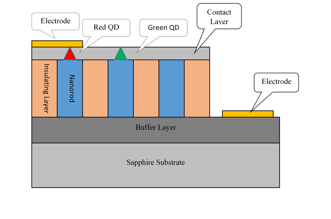
​Samsung Display (pvt) likes to hedge its bets.  While it is in the early stages of promoting and producing its QD/OLED technology, it has been researching the development of nanorods, which we first mentioned back in 2020 as a way for the company to offset the use of a fluorescent blue emitter in its QD/OLED displays.  Nanorods are small structures that are ‘grown’ using the same materials used for LEDs, and as the direction of the growth can be controlled, these structures are grown as rods, which are bunched together to form a light source, in this case a blue one.  The nanorods generate blue light which is then converted into red and green via quantum dots.  While that sounds relatively simple, getting the nanorods, which are less than 1um wide to stand up next to each other is a bit like herding cats, they tend to go in every direction, so Samsung is using a process called dielectrophoresis, similar to the process used to separate platelets from whole blood, which aligns the rods by using an electric field.  The process lines up the rods vertically, which represents a major step toward the commercialization of the process.
That said, the process is still under development, as regulating the number of nanorods in each sub-pixel is key to maintaining brightness consistency across the display, and that is just one of the issues that face SDC during the nanorod development process and expectations that SDC has solved most of the nanorod issues last year gave confidence to some that SDC would move the technology toward the development of a pilot production line this year.  It seems that SDC has decided to postpone the construction of the nanorod production line and has sent back the team that was to implement the new line to their former positions and returned the project to the R&D level.
SDC had originally planned to produce nanorod based displays sometime in 2024 or 2025 however the line postponement seems to have pushed that back a year or so, which might affect the plans of parent Samsung Electronics (005930.KS), who is looking to augment its TV lineup with more premium products, which nanorod displays would have supported.  While SDC has built a 30,000 sheet/month fab for its QD/OLED display production, thyat capacity represents only a small portion of what Samsung Electronics would need to make the technology a featured product, and while the initial reception to QD/OLED technology has been positive, without some sort of capacity expansion QD/OLED would have to remain a niche product against LG Display’s OLED TVs, which are expected to see between 9m and 10m units shipped this year.  Perhaps the postponement of the nanorod project foretells a decision by SDC to expand QD/OLED capacity, but no announcement has been made as of yet, “You are burnin’ daylight”
Picture
Nanorod Structure - Source: Samsung
0 Comments

Innolux Update

5/12/2022

0 Comments


Innolux Update
​

​Yesterday we noted the weakness at Taiwanese display producers in April, which caused all three to see declines in shipments and sales.  Innolux (3481.TT) has now given some guidance as to what it expects for 2Q, which is an increase of 7% to 9% for large panel shipments and an increase of 17% to 19% for small panel shipments.  While this sounds like a positive for the company, Innolux is also expecting a a 10% to 13% decrease in ASP, which will likely generate an operating loss.  The company also announced a 50m share buyback, which is equivalent to 0.47% of the outstanding shares and declared a dividend of 18.99% of 2021 EPS, or NT$1.05 ($0.04 US).  1Q operating p[profit was NT$2.243b ($75.186m US).
Picture
0 Comments

Destructive Math

5/12/2022

0 Comments


Destructive Math
​

The display production business is a difficult one with an almost infinite number of internal and external variables working for and against production goals.  With the obvious objective of producing the greatest number of panels possible at as high an efficiency as possible, there are trade-offs that must be made in order to maintain quality while still producing profits.  OLED technology calls for a more specialized fab, which in reality are two fabs.  The first in simplified form is the one where substrates are coated with OLED materials and encapsulated, while the second is the more conventional TFT production line that generates the electronics that trigger each OLED sub-pixel.  There are cases where these processes are done on the same substrate and ones where they are separate, but the coordination between both processes is essential to avoid bottlenecks.
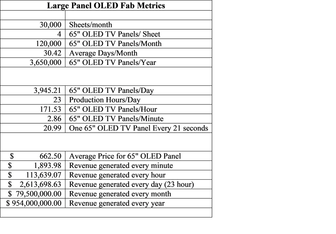
To complicate matters further, not only are such fabs massive and expensive, but they must operate efficiently at all times or the financials of the fab will be compromised, so we broke down the numbers for a typical[1] 30,000 sheet/month Gen 8.5 OLED TV panel fab to illustrate the volumes and dollars involved:


[1] LG Display is the only producer of OLED TV panels currently with Gen 8.5 fabs in South Korea and China.
Picture
​We note that these numbers represent a fab that has full utilization and 100% yield, which of course, is theoretical rather than practical, although that is the ultimate objective of every fab manager.  A new OLED Gen 8.5 fab would likely start production at a low yield, which could be anywhere from 30% to 50% depending on the experience of the engineers, with relatively rapid yield improvements for experienced producers such as LG Display (LPL), but the sensitivity to yield at these unit volumes is quite large.  A 1% improvement in yield amounts to a $795,000 gain over one month, so fab managers are extremely interested in yield improvement, especially in the early days of mass production at a new fab.  
Panels are examined at a number of points during OLED panel production to reduce the number of defective panels that pass further down the process line, particularly the deposition stage where expensive emitter materials are added.  Before deposition this is usually done through an optical process, but each fab is different in whether they use AOI (Automated Optical Inspection) tools that are in-line or tools that are off line.  In-line tools must have TACT times that are compatible with production lines or multiple tools would be necessary to alleviate bottlenecks, or the fab can choose to ‘spot check’ by taking random panels off the line for inspection, a lower cost alternative but one that could miss less frequent defects.
The testing process becomes the most sensitive right before and right after the deposition of OLED materials, as pulling a defective substrate off the line before deposition is a major cost savings, and, albeit less so, poor deposition results would prevent the panel from incurring further cost, but the tests following deposition are more complex and require more sophisticated and expensive tools that deal with particular defects that are specific to OLED, some of which require a panel to be tested using a process that changes the characteristics of the OLED materials, which makes them unusable.  Fab managers have to weigh the cost of pulling a set number of panels out of the line and destroying them to facing the chance that customers will be facing a defective panel that went undetected. 
A research team at the Korea Institute of Science & Technology (KIST) have come up with a way to test OLED panels at an ‘intermediate’ stage, meaning after deposition but before encapsulation, that is not destructive.  Testing OLED panels using a contact method is destructive but necessary, while testing them using a non-contact (UV irradiation) is also destructive, so the ‘cost’ of testing OLED TV panels is a yield reducer but carries significant financial risk if the defective panels reach consumers.  The researchers at KIST have found a way to test for defects in OLED material deposition that uses terahertz waves that do not affect the materials themselves, particularly blue OLED emitters which age faster than other OLED materials, and is therefore non-destructive. 
Terahertz waves, which are an order of magnitude higher than the gigahertz spectrum used for cell traffic, can penetrate the very thin layers of OLED materials, but are stopped by thick substances, and can be used to create high resolution images of the interior of thin films without their destruction.  If the research is able to translate these results (Yeongkon Jeong, 2022) into a practical product, it would go a long way toward improving OLED panel quality without reducing yield, and while we don’t usually note such basic research, its non-destructive characteristics make it viable for examining thin films or ultra-small structures like Micro-LEDs and is therefore extremely relevant to the display industry, regardless of how it evolves over the next few years.
0 Comments

Wolfspeed Tames the Mohawk Valley

5/11/2022

0 Comments


Wolfspeed Tames the Mohawk Valley
​

Way back in September 2019 we noted that CREE (WOLF), now known as Wolfspeed, was planning the constructing what it says is the world’s largest SiC (Silicon Carbide) production facility in Marcy, NY.  The project, which was expected to cost $1.5b (Empire State Development Fund to contribute $500m) was to be built outside of Utica on the “Marcy Nanocenter”, which is a 450 acre site close to SUNY Polytechnic Institute, considered ‘the largest shovel-ready semiconductor site in the world’ by whoever wrote the copy for the Nanocenter.  The development and construction program of the site was expected to take eight years during which CREE/Wolfspeed was to avail itself of space at the SUNY campus in Albany, using equipment that is part of the NY Power Electronics Consortium.   
About a year later we noted that CREE had decided to sell its LED products business to Smart Global Holdings (SGH) after having sold its lighting products division to Ideal Industries (pvt) in May of 2019.  It seems that Wolfspeed has completed and opened its massive 200mm SiC fab as of the end of last month.  We expect that given the initial eight year project timeline additional capacity will be added over time, but the project, which is expected to generate 600 new jobs in the region during the first 8 years of operation, has begun to run wafers and the company has signed an agreement with Lucid Motors (LCID), whose Lucid Air is said to be able to travel an EPA estimated 500+ miles on a single charge.  The new Wolfspeed fab will be providing SiC power modules to Lucid under the multi-year agreement.
Picture
Original CREE site before construction - Source: Google Earth
Picture
- Wolfspeed SiC Project in 2020 - Source: Observer-Dispatch
Picture
The completed Wolfspeed Fab - Source: Wolfspeed.com
0 Comments
<<Previous
Forward>>

    Author

    We publish daily notes to clients.  We archive selected notes here, please contact us at: ​[email protected] for detail or subscription information.

    Archives

    May 2025
    April 2025
    March 2025
    February 2025
    January 2025
    January 2024
    November 2023
    October 2023
    September 2023
    August 2023
    June 2023
    May 2023
    February 2023
    January 2023
    December 2022
    November 2022
    October 2022
    September 2022
    August 2022
    July 2022
    June 2022
    May 2022
    April 2022
    March 2022
    February 2022
    January 2022
    December 2021
    November 2021
    October 2021
    September 2021
    August 2021
    July 2021
    June 2021
    May 2021
    April 2021
    March 2021
    February 2021
    January 2021
    December 2020
    October 2020
    July 2020
    May 2020
    November 2019
    April 2019
    January 2019
    January 2018
    August 2017
    July 2017
    June 2017
    May 2017
    April 2017
    March 2017
    February 2017
    January 2017
    November 2016
    October 2016
    September 2016

    Categories

    All
    5G
    8K
    Aapl
    AI
    AMZN
    AR
    ASML
    Audio
    AUO
    Autonomous Engineering
    Bixby
    Boe
    China Consumer Electronics
    China - Consumer Electronics
    Chinastar
    Chromebooks
    Components
    Connected Home
    Consumer Electronics General
    Consumer Electronics - General
    Corning
    COVID
    Crypto
    Deepfake
    Deepseek
    Display Panels
    DLB
    E-Ink
    E Paper
    E-paper
    Facebook
    Facial Recognition
    Foldables
    Foxconn
    Free Space Optical Communication
    Global Foundries
    GOOG
    Hacking
    Hannstar
    Headphones
    Hisense
    HKC
    Huawei
    Idemitsu Kosan
    Igzo
    Ink Jet Printing
    Innolux
    Japan Display
    JOLED
    LEDs
    Lg Display
    Lg Electronics
    LG Innotek
    LIDAR
    Matter
    Mediatek
    Meta
    Metaverse
    Micro LED
    Micro-LED
    Micro-OLED
    Mini LED
    Misc.
    MmWave
    Monitors
    Nanosys
    NFT
    Notebooks
    Oled
    OpenAI
    QCOM
    QD/OLED
    Quantum Dots
    RFID
    Robotics
    Royole
    Samsung
    Samsung Display
    Samsung Electronics
    Sanan
    Semiconductors
    Sensors
    Sharp
    Shipping
    Smartphones
    Smart Stuff
    SNE
    Software
    Tariffs
    TCL
    Thaad
    Tianma
    TikTok
    TSM
    TV
    Universal Display
    Visionox
    VR
    Wearables
    Xiaomi

    RSS Feed

Site powered by Weebly. Managed by Bluehost