Supply Chain Market Research - SCMR LLC
  • Blog
  • Home
  • About us
  • Contact

China Locks down Parts of Shenzhen

8/29/2022

0 Comments


China Locks down Parts of Shenzhen
​

Shenzhen, China is the 4th largest urban city in China, with a direct population of 12.6m and an urban population of 17.6m, about the size of New York City and LA together.  The government of Shenzhen has locked down a portion of the city due to the discovery of 11 cases of COVID-19 (9 symptomatic), closing all rail and metro stations and restricting residents to one person per family able to purchase groceries or other essentials every two days, as long as they have a negative PCR test within the last 24 hours.  All businesses in the Futian and Luonu Districts have been ordered closed, although take-out restaurants are still open, but food deliveries are only allowed to be made to community lock-boxes and then picked up by residents.  Most important is the closure of the CBD (Central Business District) in the city, a 2.4 mi2 area that is home to the city government, and a wide variety of major businesses, including one of the city’s biggest electronics retailers.
To get some understanding of the size of the two districts that were closed, they are the equivalent of the size of mid-town Manhattan, in order to contain 11 COVID cases, and the cites of Xianghe (just under 400,000 residents) and Zhuozhou (~380,000 residents), were shut down last week after a total of nine cases were discovered.  Both cities are within 50 miles of China’s capital city of Beijing where residents are required to get a PCR test every three days in order to ride public transportation and enter most public buildings.  We wonder how that might work in NYC…wonder who would be checking PCR test results for those in Figure 2… 
Picture
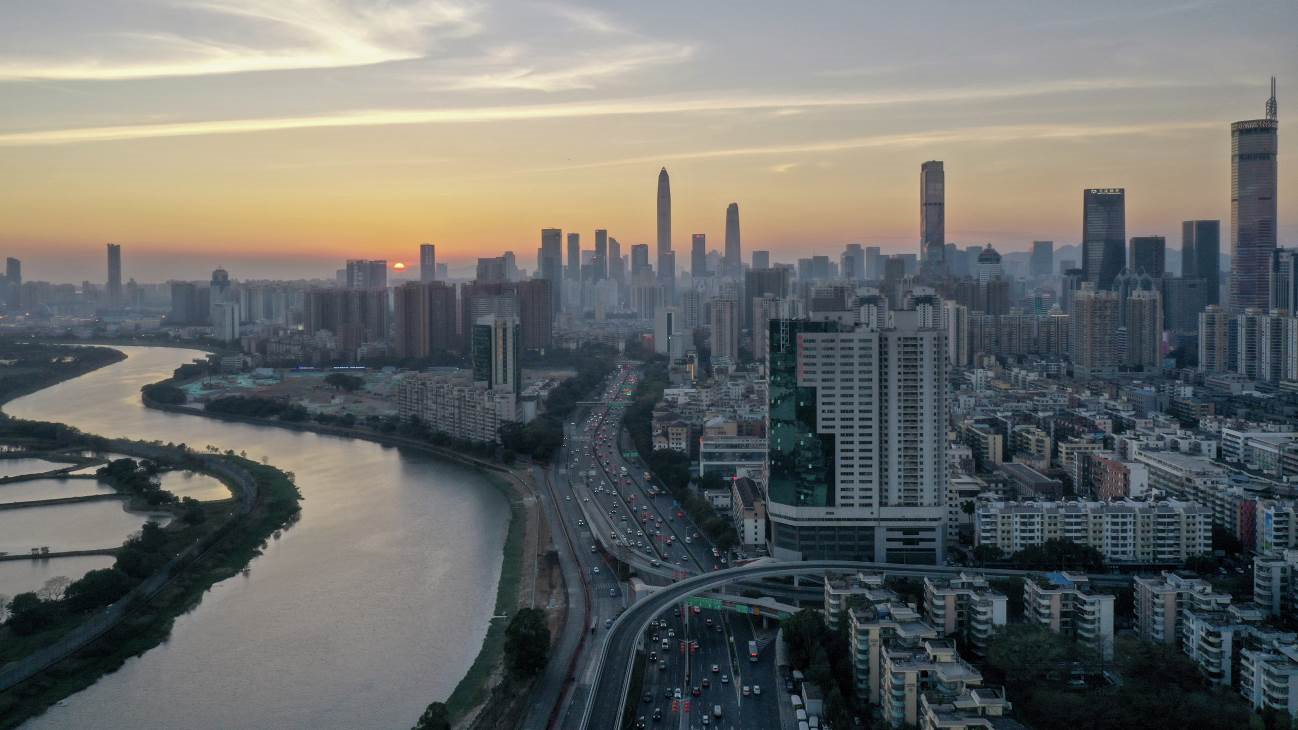
Skyline of Futian CBD - Source: By Charlie fong - Own work, CC BY-SA 4.0, https://commons.wikimedia.org/w/index.php?curid=99646288
Picture
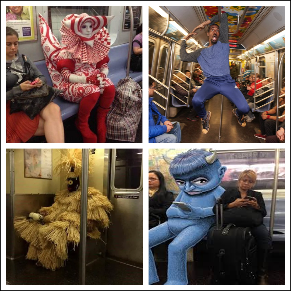
Typical NYC Subway Riders - Source: Various
0 Comments

Trade Exemptions – Between a Rock and A Hard Place

8/29/2022

0 Comments


Trade Exemptions – Between a Rock and A Hard Place
​

​While the US government seems intent on expanding trade restrictions on semiconductor equipment for Chinese foundries, it seems that they will be making exceptions for those semiconductor fabs in China that are operated by South Korean firms, Samsung Electronics and SK Hynix (000660.KS), according to an anonymous diplomatic source in Korea.  As we have previously noted, US equipment vendors have received notification from the US Department of Commerce asking them to end the sale of tools and software used in the production of chips at or under 14nm, essentially making it more difficult for Chinese OEMs to design advanced node devices and similarly making it more difficult for Chinese foundries to produce same.
While the US has already been rejecting license applications for sales of such equipment from a number of US vendors, limiting the financial impact to a degree, with US ally South Korea having two fabs on the Mainland, getting equipment to those fabs would technically violate the US trade rules, which is the reason the US has recently spoken to the South Korean government, explaining that the fabs operated by Korean firms will not face the increased restrictions being placed on Chinese semiconductor companies.  Samsung and SK Hynix both produce NAND and DRAM at the Chinese facilities, which some would consider less than advanced technology, which would likely be the official basis for the exemption, but it seems that China has little recourse regardless of the reason, as punishing Samsung and Hynix for their relationship with the US would only serve to add to the possibility that neither company will look toward expanding its footprint in China.  The Chinese trade press is making considerable noise about how the country is expanding its efforts in EDA and production tools but the development of such an industry locally will be a long one and will leave China’s semiconductor industry years behind in the development of advanced processes until successful.
0 Comments

Notebook Shipments to Get Better?

8/26/2022

0 Comments


Notebook Shipments to Get Better?
​

According to Taiwan-based Digitimes, global notebook shipments, which declined by 16% q/q and 24% y/y (our estimates differ at ↓15.0% q/q and ↓13.0% y/y in 2Q) will see shipments increase in both the 3rd and 4th quarters of this year.  The 3Q increase is expected to be 12% in 3Q and 3% in 4Q according to Digitimes as brands push volumes to meet targets, albeit targets that have been lowered recently.  Citing weakness in 2nd quarter and seasonality as the basis for the sequential increases, they see relatively little impact from the power issues in China.
As we have noted previously notebook panel shipments declined 12.2% in July as brans reduced orders to work down inventory, but we also saw little incentive for consumers to buy as prices on existing notebook inventory were high and brands seemed unwilling to offer steep discounts.  While that should change a bit this month as inventory is consumed, albeit at a relatively slow arte, it would take a strong September to meet the Digitimes goal.  We certainly don’t rule it out but look more to notebook panel shipments as early indicators of demand, even if that decline is a bit exaggerated.  We are expecting the notebook panel market to tighten a bit and panel price declines to be less than in the past few months, but until demand at the consumer level picks up, we are a bit less optimistic about seasonal growth for notebook shipments in 3Q.
Picture
Aggregate Notebook Shipments & Panel Shipments - 2Q 2019 - 2Q 2022 - Source: SCMR LLC, various
0 Comments

Blue

8/26/2022

0 Comments


Blue
​

​In our note yesterday, we mentioned Samsung Display’s (pvt) potential expansion of its QD/OLED display capacity, both through improvements in process tact time and the eventual conversion of shuttered LCD fab to additional QD/OLED lines.  Some of what we noted was derived from a recent speech made by the CEO of Samsung Display where he made a number of specific references to SDC’s plans for QD/OLED, a technology that SDC is promoting as an alternative to LG Display’s (LPL) WOLED.  The two large panel display technologies are the same in that they are both based on OLED emitters as light sources, but differ in the way that they quantify that light into Red, green, and blue sub-pixels that are necessary for full color displays.
WOLED technology uses a yellow/green (We note that yellow is a combination of green and red in light) phosphorescent OLED emitter combined with a blue fluorescent emitter as its light source.  With all three primary colors represented, the mix produces white light.  The white light is then passed through a color filter, essentially a sheet of red, green, and blue dots of phosphor materials.  The red phosphor dots allow the red component of the white light to pass through, while the green and blue dots do the same, creating an RGB pixel, one of ~8.3m on a 4K display.  While this is a cost effective way of producing an OLED TV display, as each sub-pixel blocks what is theoretically 2/3 of the light, much of the light intensity of the OLED materials is lost at the color filter.
Samsung Display uses a different technology for their QD/OLED displays.  The light source is a blue fluorescent emitter, similar to the type used in the WOLED process, but the color filter phosphors are replaced with red and green quantum dots.  Quantum dots differ from phosphors in that they do not block light, but convert it from one frequency to another, which corresponds to changing the color, so in the SDC system, in theory, the blue light is converted to red and green sub-pixels while the blue light passes through unchanged without filtering out other color components, producing a brighter display.
Both systems has a drawback, and that is they rely on blue phosphorescent emitters, which differ from phosphorescent OLED emitters in that fluorescent emitter are only able to emit 25le to generate 25% of the light that phosphorescent emitter materials can.  The physics behind this issue is complex, but if OLED panel producers had the ability to use a blue phosphorescent emitter they would, other than the fact that they are not commercially available, hence the reliance on the lower output fluorescent blue.  Again, the physics behind why a blue phosphorescent emitter is not available is complex, but leave us to say that the higher energy levels of blue phosphorescent emitters causes them to break down more quickly than red or green, and deep blue phosphorescent emitters do not yet have the lifetime needed for commercial use.
There is an alternative, which is a derivative of fluorescent blue called TADF (Thermally activated delayed fluorescence) which improves the characteristics of generic blue fluorescent emitter materials, but they are still on the cusp of having the characteristics needed for commercial display, which leaves both Samsung Display and LG Display to use fluorescent blue emitters and look for ways to improve output until a blue TADF or phosphorescent OLED emitter can be commercialized.  Universal Display (OLED) and a number of other display material suppliers have been working toward the commercialization of such a material, with UDC expecting product by 2024, along with SDC itself, who has license agreements with UDC.  Samsung recently cited its own developments in the development of a blue platinum-based phosphorescent emitter material but gave no timeline as to its potential commercialization or internal use.
Back to the speech given by Samsung Display’s CEO this week…what caught our attention was the reference he made to changing the blue fluorescent emitter material currently used in the QD/OLED process to a blue phosphorescent ar blue TADF material to increase the light emitting efficiency.  This seems to imply that SDC is considering changing the QD/OLED stack with what would have to be a commercial blue emitter that has been developed by a partner or affiliate, which would be a major step forward in the development of OLED materials.  We expect the production of such a material would be done in outside of Samsung itself, which opens the question up as to whether this material will be exclusive to Samsung or whether it will be made available to other OLED producers.  While the advantage to Samsung would be obvious if the IP is limited, the licensing of said IP would allow the OLED industry to progress further, particularly large panel; OLED devices, and would improve the characteristics of both WOLED and QD/OLED, as well as improving small panel OLED displays by increasing their efficiency and reducing power requirements.  While this was a mention in a longer speech, we see it as carrying significant weight toward the commercialization of a blue phosphorescent material.  Only 494 days to wait to see if the prediction rings true… 
0 Comments

Speaking of OLED materials…

8/26/2022

0 Comments


Speaking of OLED materials…
​

​Recent data concerning the sales of OLED materials in 2Q indicated that the industry saw a sales decline of 2.1% from the previous quarter although up 7.8% y/y.  According to UBI, a local Korean Research firm, the three largest small panel OLED producers saw declines in OLED material purchases in 2@, while OLED material for large panel displays remained roughly flat.  In order to validate that data we matched those changes to small panel OLED shipments in our database in the following table:
Picture
​According to UBI LG Display’s OLED material purchases for OLED TV production remained flat q/q in 2Q while Samsung Display’s large panel material purchases were up slightly, although considerably below those of LGD’s considering Samsung Display has limited large panel capacity for its QD/OLED displays.  We note that while sales of OLED materials at Universal Display represent only emitter materials, material sales in 2Q at UDC declined by 9.2%, although shipments to Korea (Samsung and LG) declined by 11.8% and to Customer A & Customer B, assumed to be Samsung and LG, declined by 9.2%, while BOE (Customer C) saw a decline of 6.7% q/q.  Note also that units shipped in the table above include small panel shipments only while material purchase ROC is for both small and large panel OLED displays.
While there are a  number of factors, particularly material inventory levels, that would affect OLED material purchases, the overall impact of what was a progressively more difficult quarter for the overall display space, was less so for the OLED display segment, and while we expect that the 3rd quarter will continue the weakness already seen in July for the LCD space, we expect the impact will again be less for OLED producers, especially in light of the build toward the release of the iPhone 14 series.  If you have to be producing materials for the display space, OLED is still the place to be, at least so far.
0 Comments

QD/OLED Expansion on the Cheap

8/25/2022

0 Comments


QD/OLED Expansion on the Cheap
​

The display industry is big on numbers, with one of the more important metrics being fab production capacity but a fab’s stated capacity (say 30,000 sheets/month) actually has little to do with what the fab actually produces and represents a theoretical number that is in most cases a maximum.  The most obvious factor that affects actual production vs. stated capacity is yield, which varies widely from product to product, production experience, and equipment performance at various stages of the display production process.  For OLED displays, the production process can be divided into three segments, the first being the production of the TFT (Thin-film transistor) circuitry that triggers the OLED materials to produce light, the second being the deposition of OLED materials on a substrate, and the third being encapsulating the materials and making electrical connections.
We note that TFT production is typically done on a line that is separate from the deposition line, typically run in parallel to the deposition line, and an early point at which actual production capacity begins to fall below that stated maximum is the time it takes to produce the TFT against the time it takes to produce the second step, the deposition of OLED materials.  The TFT process tends to have a shorter end-to-end process time than the deposition line, as it is based on process tools used in semiconductor manufacturing that are widely available, while OLED deposition tools are quite specific to the industry and produced by few equipment vendors, such as Sunic Systems (171090.KS), Canon-Tokki (CAJ), Dai Nippon Printing (7912.JP), and Screen Holdings (7735.JP).  Potential bottlenecks occur when TFT production must wait for the deposition process, reducing overall fab efficiency, although given the three potential TFT types used for OLED displays (LTPS, IGZO, LTPO[1]), each with its on process steps and complexity, TFT process time can vary considerably depending on the product specifications.
There are a number of steps that occur before a substrate gets to the deposition line, including detailed optical inspection, a number of cleaning steps, the coating of a layer of Indium Tin Oxide (ITO) that will become the anode of the OLED stack, and laminating the flexible substrate to a rigid glass sheet to keep it stable during processing.  The substrates are loaded into a robotic system that performs additional cleaning and then moved by another robot to a chamber that deposits HIL (Hole-Injection Layer) materials.  When that process is completed the robot moves the substrate to another chamber where HTL materials (Hole Transport Layer) are deposited, followed by three individual steps where red, green, and blue OLED materials re deposited.  Each of these deposition steps is done through a fine metal mask, essentially a screen that keeps each pixel or sub-pixel spaced correctly.  Following the deposition of the three OLED emitters, the substrate moves to chambers that deposit ETL (Electron Transport Layer) and EIL (Electron Injection Layer) materials.
We note that all of these deposition processes must take place in a non-reactive atmosphere, which is commonly Nitrogen, as exposure to even minute amounts of oxygen or water vapor will erode OLED materials and cause the substrate to be discarded, and a number of processes are done under high vacuum conditions, so there is considerable cycle time for reducing pressure and heating chambers for each step.  Once the substrate has completed these steps it remains in the enclosed atmosphere and is encapsulated either with a sheet of glass sealed with glass frit[2] or through the deposition of alternating layers of transparent organic and inorganic materials.
The deposition system shown in Figure 1 is designed for Gen 2 substrates which are 1.87 ft2, which allows the chambers to be relatively small.  Typical OLED production systems are designed to handle Gen 6 substrates, which are 29.86 ft2, although such substrates are typically processed after being cut in half or in quarters, keeping the chamber size as small as possible.  These systems cost hundreds of millions of dollars depending on the configuration and given the small number of suppliers, lead times are between 9 months and 18 months, so considerable planning is needed to get the equipment to a new line and brought up to production specifications, but more importantly is cycle time, which in the case of the tool below is between 3 to 5 minutes/substrate for a single stack structure of this size, and that does not consider any additional layers that particular producers add to differentiate their product.  Such a system can run almost continuously for ~5 days, at which point chambers must be cleaned and masks replaced, at which point the system has to be restarted, recalibrated, and tested before it is put back in production.
Even this cursory OLED process explanation shows the many points at which the process tact time can get extended, reducing output based on the equipment and process alone, and then comes yield, which is the variable that can be the difference between an OLED fab being profitable or not profitable.  Once the OLED displays come out of the encapsulation process, they are tested.  This is done visually (automated) where physical defects are tagged, electrically, to make sure each sub-pixel is able to turn on and off, and characteristically, where luminance, color point, and uniformity are checked.  Some discrepancies that appear between sub-pixels can be corrected by adjusting electrical values, while others cause the OLED panel to fail and be binned for possible repair.  OLED process engineers look for problems that are causing panels to fail testing procedures, and whether they are ‘one-time’ issues or whether they are recurring, and if they are recurring, is it an problem that is occurring at the same point in each display or more random. 
By assessing the test data engineers can determine the source of the problem and make adjustments quickly in order to maintain acceptable yields, especially at the beginning of a new product run or near the end of a use/clean cycle, and when one looks at an OLED line that is capable of producing 15,000 Gen 6 substrates/month or ~1 55” panel/minute, every 1% drop in yield equals ~$73,000/ month in lost sales[3].  It is therefore incumbent on OLED panel producers to watch and improve yields regardless of product in order to achieve profitability.  But what if you have already improved yields and you are still below the quota needed to supply customers?  Typically panel producers begin planning for a new fab, which is an 18 to 20 month process and costs upwards of $3b, a solution that is acceptable on a long-term basis but does little in the near-term.  That said, Samsung Display (pvt) has come up with another, far less expensive solution that goes a long way toward solving the problem.
Samsung Display has developed a large panel display production process that combines the positive aspects of OLED materials and those of quantum dots.  By using quantum dots to shift the color of blue/green OLED emitters to red and green, they avoid the use of a color filter that reduces the light output of WOLED displays produced by LG Display (LPL).  The process is new and still being refined, even as the company is in production, but SDC’s concern (and that of their customers who are Samsung Electronics (005930.KS), Sony (SNE), Dell (DELL), and MSI (2377.TT)) was that they would not be able to produce enough QD/OLED displays to satisfy customer demand, as they have a single Gen 8 production fab for this new product line.  This was especially onerous when the line first went into production as yields were ~50%, meaning they tossed one panel for every two they produced, but SDC was able to bring that yield up to an acceptable 85% by mid-year.  However bringing yields from 50% to 85% is far easier than bringing it from 85% to 90% and that difference in unit volume would not be enough to fill the product gap they see coming, so SDC is working to change the other variable in their QD/OLED production process, that of tact time.
According to sources in South Korea, Samsung Display has set the goal of increasing output of its QD/OLED line by 30% by the end of the year by reducing bottlenecks that keep tact time high.  This would imply a similar reduction in tact time, not an easy task, but one where SDC has the advantage of being the only producer of QD/OLED and has had more experience with RGB OLED production than any other OLED supplier, including LG Display, who is the only global supplier of WOLED TV panels.  As the WOLED process uses conventional phosphors to filter the white OLED light into primary colors, the process differs from SDC’s large panel QD/OLED process, and from the basic RGB OLED process described above, but Samsung’s expertise and close connection to its OLED equipment suppliers gives them the opportunity to increase volume and sales without building out new capacity in the near-term, albeit a short-term solution. 
We expect that SDC has already made the decisions necessary to begin planning for additional QD/OLED capacity, although this has not been an ideal time to be making such plans, which will likely be implemented in one of the company’s shuttered LCD fabs, but as noted this will take considerable time, so such an interim solution is like adding half of a 15k production line for free and one that likely put SDC upper management and that of parent Samsung Electronics in a happier state of mind, something in short supply across the CE space currently.  Now they have 128 days in which to do it…


[1] LTPS – Low Temperature Poly-silicon
IGZO – Indium Gallium Zinc Oxide (aka ‘Oxide’)
LTPO – Low Temperature Poly-silicon Oxide

[2]  Glass frit – a low melting point glass powder mixture that can be used to seal or bond glass to glass or other materials, essentially a glass solder.

[3] Assuming a generously low $160 cash cost
Picture
Canon-Tokki ELVES OLED Mass Production System - Source: Canon-Tokki
0 Comments

Innolux ‘Encourages’ Employees to Take ‘Vacations’

8/24/2022

0 Comments


Innolux ‘Encourages’ Employees to Take ‘Vacations’
​

​Innolux (3481.TT) is one of almost all large panel LCD producers that have lowered utilization rates as the display industry finds itself with high inventory levels and decreasing demand.  Given that panel producers do not want to fire workers that have been trained only to hire and train new workers when utilization rates move up, the company has announced a new ‘Unified Vacation Plan’ for employees that designates September 12th and 13th as ‘vacation days’, along with October 5th, 6th, and 7th, with the payroll system deducting said ‘vacation days’ from worker’s pay, which has caused workers to complain to the media and the Taiwan Ministry of Labor.
The Ministry of Labor seems to believe that the Innolux leave announcements ‘clearly violate Labor Standards Law’ and put the company in position to receive a maximum fine of NT$1,000,000, which is the equivalent of ~$33,000 US$.  The average engineer in Taiwan earns $85,300/year, which comes to $234/day and assuming all 52,600 Innolux employees are forced to take the 5 additional unpaid vacation days, the savings to the company would be ~$62.5m, which makes a $33k fine seem a bit insignificant.  Of course it does little for company/employee relations but with the outlook cloudy for the next few months we expect management would not be distressed if a few employees left for greener pastures.
0 Comments

Huawei Founder Changes Priorities

8/24/2022

0 Comments


Huawei Founder Changes Priorities
​

The founder of China’s largest telecommunications company Huawei (pvt) is usually optimistic about the future of his company and the prospects for global technology, although having been in the sights of the US government’s trade war with China have made an impact on the founder’s positivity as those trade restrictions forced the company to move away from its more traditional products and find areas where it is not dependent on technology that is US based or US developed.  It seems that not only is Ren Zhengfei concerned about the company’s ability to navigate the enormous roadblocks the US has set up, but in an internal network staff meeting he indicated that it is time for the company to change direction from its previous growth mode to one of ‘survival’, emphasizing profit and cash flow.
He explains that the global economy is headed for a decade of weak demand, particularly during the 2023 – 2024 period, and is concerned that the company can survive in such an environment.  In order to stave off any possibility of such an occurrence, he wants to end all complex projects and abandon businesses that have little chance of becoming profitable, reduce R&D on projects, such as electric vehicles, that could take many years to develop, and refocus the company on IT infrastructure and customer service.  While he admitted that his pessimistic view was colored by the US sanctions, the war in Ukraine, inflation, and a post-COVID world, the company’s 1H results saw little growth and a large drop in profitability, with the slowdown in demand across the company’s device businesses taking a toll while the IT business remained a growth driver.
It was also mentioned that Huawei could abandon markets in certain countries and face the fact that survival is now the focus, which means trimming the 2023 budget, reducing ‘scientific research’ and emphasizing a few key areas where component and product development can be linked together, and above all, employees should not ‘tell stories’ about the potential for projects and present a realistic prediction of prospects as ‘company losses will be deducted from your food (pay) package”.  From an expense perspective he wants only two categories, paying stable wages to employees and paying back bank loans, while indicating that bonus assessment this year and next will be based more on operating profit as an encouragement to employees to drive profits and less on reducing the wage gap across the company
All in, this more focused and lean Huawei is long overdue, and while the company has taken measures to counteract the US trade sanctions, there was still a focus in the fact that Huawei is China’s largest privately-owned patent holder and that the company and China itself takes pride in the fact that the country’s R&D spending this year will be larger than that of the US for the first time.  For a company so enmeshed in global politics, such focus is a distraction and while naysayers will cite the necessity for deep scientific research to create long-term product strategies, cutting the budgets on all but those with the highest probability for profits is what will keep Huawei from drifting toward its own demise. 
When the initial sanctions were placed on the company in August 2018 there was a ‘doesn’t matter’ attitude from management, which became a ‘hunker down’ philosophy about a year later as the US tightened the trade noose, but there has been a lack of understanding by senior management as to the fact that despite its former size and stature, the company could implode or slowly drift into oblivion.  Hopefully these words from the company’s founder will have an impact on both management and rank-and-file workers and will snap them out of the ‘too big to fail’ mantra that can easily become a psychological barrier to preventing just such an occurrence.   If Mr. Zengfei is even half right about the prospects for the next few years Huawei needs to ‘get it’s mind right’ if it does not want to join the list of those companies that didn’t and no longer exist.
Picture
0 Comments

Samsung Commits to New OLED Fab

8/24/2022

0 Comments


Samsung Commits to New OLED Fab
​

The CEO of Samsung Display (pvt), affiliate of Samsung Electronics (005930.KS), indicated that it will be building a Gen 8 OLED fab in its production complex in Asan, South Korea, designed for the production of IT OLED panels.  As we have noted previously (8/16/21, 06/30/22,5/26/22), the construction of such a facility has been rumored, particularly as SDC has been developing specialized OLED deposition equipment with tool supplier Ulvac (6728.JP) that will help overcome the physical limitations that restrict the use of fine metal masks to Gen 6 OLED fabs.  Fine metal masks are used to pattern OLED emitter materials on rigid or flexible substrates but begin to sag, causing defects, when they are used above Gen 6.  The new process that SDC is developing places the deposition chamber and the masks vertically, rather than horizontally, keeping gravity from deforming the masks.
We expect the fab will be built in the L8 building, where SDC formerly had two large LCD fabs, producing up to 350,000 sheets/month at its peak, or the equivalent of 25.2m 55” LCD TV panels/year.  SDC closed the first line in 2019, sold the equipment to Chinese LCD module producer Shenzhen Efonlong (pvt), and since built the production line for the company’s QD/OLED display products in that location.  While no specific details about the new fab’s capacity were given, the company is expected to begin production on the new line in 2024, which will improve the efficiency of OLED panel production for IT products (monitors and notebooks), which are currently being produced on less efficient Gen 6 OLED fabs at SDC.  This would coincide with Apple’s (AAPL) rumored plans to move the iPad from LCD to OLED displays in that year.
The OLED IT category is small relative to OLED smartphones, watches, and TVs, but represents a less competitive category and rapid growth. Current estimates see OLED monitor revenue growing from $57m last year to over $200m this year, although that includes QD/OLED and OLED notebooks growing almost 40% in sales y/y and over 60% in units.  The chairman also indicated that SDC would be pursuing two forms of micro-displays, micro-OLED and micro-LED, neither of which comes as much of a surprise considering Samsung’s micro-LED commercial products are already available albeit at extremely high prices.  The indication was that the company will be in mass production of micro-displays in the 2024 year along with the Gen 8 OLED IT line, which musts some significant milestones for SDC over the two years.  While SDC management did not indicate the cost of these projects, the Gen 8 fab alone is estimated to cost between $2.3b and $3b, and we would expect that the OLED micro-displays would be produced on silicon, which would entail a dedicated production line. 
All in, these are big projects but necessary for SDC to maintain its leadership role in the RGB OLED space and compete for micro-LED commercialization with Chinese panel producers, who have also been making such investments.  While 2023 will be a year primarily dedicated to more traditional OLED products, which are increasingly influenced by macro factors, 2024 and 2025 will be years in which SDC is able to expand its display product line, particularly with new premium priced display products that will lessen its exposure to competition from Chinese panel producers.  There are still a large number of roadblocks to overcome but it is nice to have the backing of one of the world’s largest CE companies when it comes to taking such chances.
Picture
Samsung Asan Fab Complex - Source: SamMobile
0 Comments

Lead-Times Getting Shorter

8/24/2022

0 Comments


Lead-Times Getting Shorter
​

​Lead-time and supply issues in the semiconductor space have been a thorn in the side of fabless IC chip houses since the pandemic began, and the cause of sales shortfalls and missed performance goals.  Foundries, with only limited near-term capacity expansion possibilities, rationed production, causing buyers to double order to gain leverage with silicon suppliers.  In many cases foundries are still running at full capacity, but as demand for CE products has dwindled, particularly smartphones, chip suppliers that feed the smartphone supply chain are no longer double ordering, and in some cases are cutting back to work down existing inventory.   
Recent comments from a number of network and RF equipment suppliers in Taiwan have indicated that lead times have fallen from a high of 50 weeks to a mere 30 weeks, allowing those that had been limited by foundry supply constraints in the 1st half of the year, to bring their customer fulfillment rates up by 10% or more, even as the silicon market remains tight.  While a number of such companies that were supply limited in 1H now expect to see better performance in 2H as lead times decrease and transportation costs come down a bit, with higher fulfillment rates at Unizyx (3704.TT), Sercomm (5388.TT) and Arcadyan (3596.TT) in Taiwan. 
However not everyone is a beneficiary, as Qurvo (QRVO) indicated on their quarterly call.  The company was forced to pay foundry UMC (UMC) $110m to satisfy what was essentially a take-or-pay contract that was put in place last year to ensure the company had a guaranteed share of UMC’s capacity.  As smartphone demand weakened, demand for Qorvo’s Wi-Fi and UWB (Ultra-Wideband) ICs did the same and the company was forced to reduce orders that put it below the contract minimum, triggering the payment.  UMC however still seems to be running at full capacity as other customers fill the gap.  Those agreements and double ordering that seemed so necessary ( and rightly so) last year and earlier this year are now coming back to bite the buyers while those that had to settle for revenue shortfalls due to supply constraints in the past are now getting close to meeting customer demand.  Now we just have to watch foundry results to see if the ‘slowness’ continues to trickle down.
 
0 Comments
<<Previous
Forward>>

    Author

    We publish daily notes to clients.  We archive selected notes here, please contact us at: ​[email protected] for detail or subscription information.

    Archives

    May 2025
    April 2025
    March 2025
    February 2025
    January 2025
    January 2024
    November 2023
    October 2023
    September 2023
    August 2023
    June 2023
    May 2023
    February 2023
    January 2023
    December 2022
    November 2022
    October 2022
    September 2022
    August 2022
    July 2022
    June 2022
    May 2022
    April 2022
    March 2022
    February 2022
    January 2022
    December 2021
    November 2021
    October 2021
    September 2021
    August 2021
    July 2021
    June 2021
    May 2021
    April 2021
    March 2021
    February 2021
    January 2021
    December 2020
    October 2020
    July 2020
    May 2020
    November 2019
    April 2019
    January 2019
    January 2018
    August 2017
    July 2017
    June 2017
    May 2017
    April 2017
    March 2017
    February 2017
    January 2017
    November 2016
    October 2016
    September 2016

    Categories

    All
    5G
    8K
    Aapl
    AI
    AMZN
    AR
    ASML
    Audio
    AUO
    Autonomous Engineering
    Bixby
    Boe
    China Consumer Electronics
    China - Consumer Electronics
    Chinastar
    Chromebooks
    Components
    Connected Home
    Consumer Electronics General
    Consumer Electronics - General
    Corning
    COVID
    Crypto
    Deepfake
    Deepseek
    Display Panels
    DLB
    E-Ink
    E Paper
    E-paper
    Facebook
    Facial Recognition
    Foldables
    Foxconn
    Free Space Optical Communication
    Global Foundries
    GOOG
    Hacking
    Hannstar
    Headphones
    Hisense
    HKC
    Huawei
    Idemitsu Kosan
    Igzo
    Ink Jet Printing
    Innolux
    Japan Display
    JOLED
    LEDs
    Lg Display
    Lg Electronics
    LG Innotek
    LIDAR
    Matter
    Mediatek
    Meta
    Metaverse
    Micro LED
    Micro-LED
    Micro-OLED
    Mini LED
    Misc.
    MmWave
    Monitors
    Nanosys
    NFT
    Notebooks
    Oled
    OpenAI
    QCOM
    QD/OLED
    Quantum Dots
    RFID
    Robotics
    Royole
    Samsung
    Samsung Display
    Samsung Electronics
    Sanan
    Semiconductors
    Sensors
    Sharp
    Shipping
    Smartphones
    Smart Stuff
    SNE
    Software
    Tariffs
    TCL
    Thaad
    Tianma
    TikTok
    TSM
    TV
    Universal Display
    Visionox
    VR
    Wearables
    Xiaomi

    RSS Feed

Site powered by Weebly. Managed by Bluehost