Micro-LED Breakthrough?
There are many issues facing the development of Micro-LED displays, with transferring the millions of tiny LEDs from wafers to display substrates. As there are almost 25m individual LEDs in a 4K micro-LED display and over 99.5m in an 8K Micro-LED display, moving such vast numbers of ultra-small devices presents some unusual challenges. That said, aside from the huge numbers, the fact that even at .99999% yield, there would be 249 and 996 non-working Micro-LEDs that would have to be individually repaired, a process that we estimate could be as costly as the entire transfer process, and yields are far from 5 9’s currently. The most recent estimates we have seen indicate that repairing each non-working Micro-LED takes about a second which would imply a 90% yield would generate 9.953m bad die for each display. At 1 second each to repair, it would take 115.2 days for repair all non-working die! There are systems that are being developed that can test all of the die that have been transferred and through various means, such as laser ablation, remove and replace the non-performing Micro-LEDs, but there is also another way.
Instead of pulling all of the die from the wafers on which they were produced, by testing the die at the source, a KGD map (Known Good Die) can be generated, which will point out those die that should not be addressed by the transfer tool, reducing the number of non-performing die that need to be reworked. Notice we said reduce, because the testing and transfer processes themselves can also damage the Micro-LEDs, however pre-testing and creating a die map can reduce the time to transfer and repair substantially. Electrically testing these tiny LEDs at the wafer level means they have to be connected to a testing probe, and with the size of Micro-LEDs decreasing toward single digit ums, this can be a somewhat destructive process for a small number of the Micro-LEDs under test, which lessens the effectiveness of the pre-transfer process. Some companies, such as Instrument Systems (4902.JP) and InZiv (pvt) test at the wafer level using optical means, which avoids the probe issues, and can both mark non-performing Micro-LEDs on the KGD map and indicate whether die metrics, such as photoluminescence (which does not need direct die contact) are up to necessary standards. That said, testing photoluminescence only can miss some metric that can only be tested by direct contact, so while a single test type system is helpful, it does not solve all of the testing and transfer issues.
According to South Korea’s Top Engineering (065130.KS), while testing for both electrical and optical characteristics at the wafer level, they have found a way to test same without direct chip contact, which, if true, would reduce the potential testing damage completely and speed up the entire production process. The tool, known as TNCEL-W can inspect Micro-LEDs at 50um or less at the wafer stage and while the company has said that they are currently conducting performance tests with domestic and foreign customers they believe they can make a significant impact on the cost of the Micro-LED process. There is little other information concerning the tool, as it is still in the test mode, but if Top has found a way to do non-destructive optical and electrical testing they could pull in the Micro-LED timeline when the tool goes into commercial production. There are still many other challenges that have to be resolved in order to make commercial Micro-LED production competitive, but we are always on the look-out for those that say they can make a dent in the Micro-LED ‘punch list’. If Top has found a way to do what they say, they have made a big step forward in the Micro-LED world.
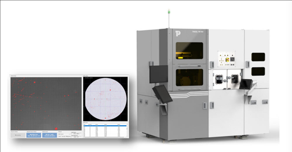
Top Engineering –TCNCEL-W – Source: Top Engineering


 RSS Feed