Glass Half Full
What do PCBs and glass have in common? PCBs have glass fiber in them, but the commonality stops there, at least for now. In this note we take a quick look at the use of glass as a core ingredient in future PCBs and as a key material for advanced semiconductor packing in the future. The unique characteristics of glass allow it to solve a number of current and future issues with semiconductors and board level products that suddenly have become high priority issues as AI creates demand for servers and high-speed silicon devices at a rapid pace. Before going further it is important to understand the basics about PCBs.
What is a PCB?
What is a PCB?

PCBs (Printed Circuit Boards) are typically made of FR-4[1], a widely used laminate consisting of a glass fiber reinforced epoxy, and copper foil, layered with an adhesive. They can be single or multi-layer (up to over 30 layers). FR-4 is inexpensive, has been standardized since the 1960’s and provides a rigid and stable framework for components, along with the ability to provide a structure for intricate traces (the equivalent of wires on a PCB) for component connections and power sources in most environments. However as the number of layers and components increases so does crosstalk (the bleed of a signal from one part of the board to another) as does the amount of heat generated, and that heat reduces the life of board components.
While PCBs have been used for many years, the demands of modern servers, especially high powered GPUs used for AI training and inference have pushed the limits of this medium and research is being done on using glass as a substrate for a number of reasons.
Unfortunately, there are drawbacks with using glass as a PCB substrate or in advanced semiconductor packaging. While FR-4 has been used for over 50 years and is well ingrained in the electronics production ecosystem, glass is a new material for these uses and has some unique manufacturing challenges.
Specialty Glass Manufacturers
This category is divided into two segments. Those large commercial glass producers that are developing specialty glass for substrates and advanced semiconductor packaging, and those suppliers who are singly focused on this particular application. While the most noise will come from the first category, it will take years for glass substrates to become meaningful in light of the other income streams these manufacturers have. That is not to say it won’t become meaningful, only that it will take years to grow the application and the ecosystem. Smaller suppliers, particularly Absolics, have been laying the groundwork for the industry, along with Intel.
Large Commercial Suppliers:
All of the companies listed under ‘large commercial suppliers’ are currently producing specialty glass products for advanced semiconductor packing R&D. Most are at the qualification level as full scale packaging using glass substrates is just beginning to materialize.
Corning (GLW)
AGC (5201.JP)
Schott (pvt)
Hoya (7741.JP)
Nippon Electric Glass (5214.JP)
Small Focused Suppliers
These companies are more focused on the substrate glass market without the distraction of much larger other businesses and have a better chance to come up with specific solutions, as long as they are amply funded.
Absolics (011790.KS)
Plan Optik (P40.XE)
JNTC (204270.KS)
Equipment Suppliers
These companies are modifying existing tools and developing new ones that allow both glass producers and fabricators to utilize glass substrates. As the technology is changing rapidly, there is no standardization on new tools at this time
LPKF Laser AG (LPK.XE)
Canon (7751.JP)
Yield Engineering Systems (pvt)
Applied Materials (AMAT)
Fabricators
These companies take th raw materials and create glass substrates to specification. This is custom work and will likely remain so for the near future, which leaves open the expansion of the list to include a much larger base.
Samsung Electro-Mechanics (009150.KS)
Intel
Assembly & Test
Component placement (assembly) will be shared between fabricators and outsourced assemblers, while we expect test (other than at the line level) to be entirely outsourced to guarantee independence and impartiality.
ASE Group (ASX)
Amkor Technology (AMKR)
Powertech technology (6239.TT)
Toray Engineering (3402.JP)
A Deeper Look - Absolics
Absolics was created as an affiliate of SKC Ltd (011790.KS) in late 2021, with SKC being one of dozens of recognizable companies in Korea under the SK Group[3] umbrella. Absolics was created to focus specifically on glass core substrates and to eventually become the world’s first large scale commercial manufacturer of glass core substrates. By exploiting the characteristics of the company’s specialty glass formulations the company expects to solve many of the issues that limit chip-level progress. The company has indicated that the use of its materials can provide up to a 50% power reduction and a 30% improvement in signal performance, which are two big issues for server farms.
The company began constructing on a $600m ~10,000 ft2 facility (Phase 1) at SKC’s campus in Covington, GA in November of 2022. The first phase of the construction was a $240m small volume glass manufacturing facility, followed by a $360m high volume line. The company received approval for up to $75m[4] in CHIPS Act funding for the phase 2 (120,000 ft2 total) facility in May of last year and up to $100m for R&D from the federal government’s National Advanced Packaging Manufacturing Program. The government weighed the cost of building a glass substrate manufacturing facility from scratch and the administrative delays associated with such a project and made the investment with a highly experience manufacturer instead. The company has targeted mass production by the end of this year with phase 1 production of 12,000 m2/year and 72,000 m2/year when phase 2 is completed,
The core of Absolics technology is its TGV (Through Glass Via) technology. These ‘tunnels’ through the glass substrate provide inter-layer communication and further reduces signal loss by reducing the overall length of the signal path through layer stacking. As chip production becomes more complex with multi-layer boards and interconnected chiplets the necessity to reduce signal interference and loss through vias and low loss materials becomes essential. This is particularly important in relation to power, which has to be delivered both horizontally across each layer and vertically to all layers and to passive components that can be embedded into the glass substrate itself.
[1] FR stands for Fire Retardant while the 4 is a designation for the grade of the epoxy-glass laminate.
[2] Silicon ~2.6 ppm/°C; Glass – 3.2 to 7.5 (adjustable)
[3] Sk Telecom – the #1 telecom company in Korea; Sk Hynix the 3rd largest semiconductor company world-wide; SK Silton the only silicon wafer manufacturer in Korea to name a few
[4] NIST indicates that Absolics has been approved for $100m in CHIPS funding, which we believe is for R&D.
While PCBs have been used for many years, the demands of modern servers, especially high powered GPUs used for AI training and inference have pushed the limits of this medium and research is being done on using glass as a substrate for a number of reasons.
- As board density increases, trace line widths decrease, making the lithography that produces these lines more difficult. While PCB boards are rigid to a degree they have inherent flexibility and not necessarily perfectly flat and when it comes to lithography, even a small change in any direction, such as a slight bend in the substrate, can cause a defect that can lead to later issues or an outright board rejection. Glass is over 1,000 times flatter than a typical FR-4 PCB.
- Thermal Expansion (CTE) occurs as the temperature rises in a material. Glass has a CTE that is similar to that of silicon, which means it expands and contracts at roughly the same rate[2], while standard PCB CTE is 2 to 3 times higher, meaning it can expand and contract at a greater rate than the components. This mismatched expansion can lead to solder joint fatigue or more serious warpage issues.
- In typical server operation, both the copper traces and the FR-4 absorb some of the signal. As boards get larger that loss increases. It also increases as the frequency of the signal increases, which becomes a significant factor with HBM (High Bandwidth Memory and High speed GPUs. Dielectric loss for glass is half to ¼ that of FR-4, and specialty glasses can reduce that loss by another order of magnitude.
Unfortunately, there are drawbacks with using glass as a PCB substrate or in advanced semiconductor packaging. While FR-4 has been used for over 50 years and is well ingrained in the electronics production ecosystem, glass is a new material for these uses and has some unique manufacturing challenges.
- Glass is brittle and fragile and can be damaged during handling and processing, lowering yield and requiring more expensive handling equipment.
- Vias, copper clad tunnels that connect layers and vent heat, are more difficult to produce than with FR-4. Lasers or ion etch is used to create vias in glass substrates, a slower and certainly more expensive process than the drilling used with FR-4 PCBs.
- The cost of substrate quality glass is considerably higher than FR-4 and the number of suppliers is extremely limited currently.
- The thermal characteristics of glass are such that it is a poor heat conductor, and as such, thermal management, already an issue with high-speed servers, becomes more so.
- Specialty Glass Manufacturers
- Equipment Suppliers
- Fabricators
- Assembly & Test
Specialty Glass Manufacturers
This category is divided into two segments. Those large commercial glass producers that are developing specialty glass for substrates and advanced semiconductor packaging, and those suppliers who are singly focused on this particular application. While the most noise will come from the first category, it will take years for glass substrates to become meaningful in light of the other income streams these manufacturers have. That is not to say it won’t become meaningful, only that it will take years to grow the application and the ecosystem. Smaller suppliers, particularly Absolics, have been laying the groundwork for the industry, along with Intel.
Large Commercial Suppliers:
All of the companies listed under ‘large commercial suppliers’ are currently producing specialty glass products for advanced semiconductor packing R&D. Most are at the qualification level as full scale packaging using glass substrates is just beginning to materialize.
Corning (GLW)
AGC (5201.JP)
Schott (pvt)
Hoya (7741.JP)
Nippon Electric Glass (5214.JP)
Small Focused Suppliers
These companies are more focused on the substrate glass market without the distraction of much larger other businesses and have a better chance to come up with specific solutions, as long as they are amply funded.
Absolics (011790.KS)
Plan Optik (P40.XE)
JNTC (204270.KS)
Equipment Suppliers
These companies are modifying existing tools and developing new ones that allow both glass producers and fabricators to utilize glass substrates. As the technology is changing rapidly, there is no standardization on new tools at this time
LPKF Laser AG (LPK.XE)
Canon (7751.JP)
Yield Engineering Systems (pvt)
Applied Materials (AMAT)
Fabricators
These companies take th raw materials and create glass substrates to specification. This is custom work and will likely remain so for the near future, which leaves open the expansion of the list to include a much larger base.
Samsung Electro-Mechanics (009150.KS)
Intel
Assembly & Test
Component placement (assembly) will be shared between fabricators and outsourced assemblers, while we expect test (other than at the line level) to be entirely outsourced to guarantee independence and impartiality.
ASE Group (ASX)
Amkor Technology (AMKR)
Powertech technology (6239.TT)
Toray Engineering (3402.JP)
A Deeper Look - Absolics
Absolics was created as an affiliate of SKC Ltd (011790.KS) in late 2021, with SKC being one of dozens of recognizable companies in Korea under the SK Group[3] umbrella. Absolics was created to focus specifically on glass core substrates and to eventually become the world’s first large scale commercial manufacturer of glass core substrates. By exploiting the characteristics of the company’s specialty glass formulations the company expects to solve many of the issues that limit chip-level progress. The company has indicated that the use of its materials can provide up to a 50% power reduction and a 30% improvement in signal performance, which are two big issues for server farms.
The company began constructing on a $600m ~10,000 ft2 facility (Phase 1) at SKC’s campus in Covington, GA in November of 2022. The first phase of the construction was a $240m small volume glass manufacturing facility, followed by a $360m high volume line. The company received approval for up to $75m[4] in CHIPS Act funding for the phase 2 (120,000 ft2 total) facility in May of last year and up to $100m for R&D from the federal government’s National Advanced Packaging Manufacturing Program. The government weighed the cost of building a glass substrate manufacturing facility from scratch and the administrative delays associated with such a project and made the investment with a highly experience manufacturer instead. The company has targeted mass production by the end of this year with phase 1 production of 12,000 m2/year and 72,000 m2/year when phase 2 is completed,
The core of Absolics technology is its TGV (Through Glass Via) technology. These ‘tunnels’ through the glass substrate provide inter-layer communication and further reduces signal loss by reducing the overall length of the signal path through layer stacking. As chip production becomes more complex with multi-layer boards and interconnected chiplets the necessity to reduce signal interference and loss through vias and low loss materials becomes essential. This is particularly important in relation to power, which has to be delivered both horizontally across each layer and vertically to all layers and to passive components that can be embedded into the glass substrate itself.
[1] FR stands for Fire Retardant while the 4 is a designation for the grade of the epoxy-glass laminate.
[2] Silicon ~2.6 ppm/°C; Glass – 3.2 to 7.5 (adjustable)
[3] Sk Telecom – the #1 telecom company in Korea; Sk Hynix the 3rd largest semiconductor company world-wide; SK Silton the only silicon wafer manufacturer in Korea to name a few
[4] NIST indicates that Absolics has been approved for $100m in CHIPS funding, which we believe is for R&D.
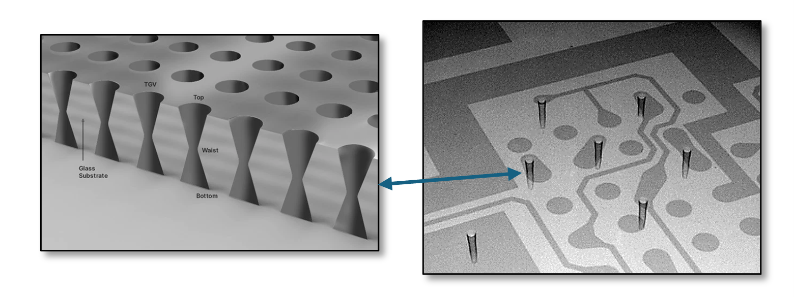
Figure 2 - Through Glass Vias - Source: Semiconductor Engineering, AGC
The research grant mentioned above is specifically targeted to TGV development in order to reduce the challenges associated with TGVs and to develop the specialized equipment to facilitate their production. This is also an extension of the company’s collaboration with the DOD under their SHIP Program (State-of-the-Art Heterogeneous Integrated Packaging) which requires ultra-low loss package designs. The company also benefits from a 12% investment SKC has made in Chipletz (pvt), a fabless substrate start-up in Texas.
The company is positioning itself as a neutral supplier to both major foundries and to design houses that do not want to purchase glass from competitors. There are others who are developing similar technology and products with internally developed expertise, such as Samsung (005930.KS) and LG Innotek (011070.KS) so it will not be without risk for Absolics, but they have partnered with over 30 suppliers and external resources in order to compete more effectively, and continue to have the backing of SK Group, the 2nd largest manufacturing company in South Korea (Samsung is 1st). There are still a number of major challenges that need to be reduced or eliminated, particularly low TGV yield and reliance on AI demand, but if glass substrates perform as well as expected in real world use, Absolics will directly benefit.
As Absolics is more focused on chip level and packaging glass substrates than board level products, we compare the parameters of using glass core substrates in advanced packaging against typical ABF and silicon interposers.

As with all new technologies, estimates vary considerably, with estimates for market size ranging from $4.3b to $7.8b in 2024 and $8.3b to $12.3b in 2032, with CAGR ranging from 3.6% to 7.8%. That said we expect there is little commonality between these estimates as the term ‘Glass Substrates’ is far to general to mean only high purity glass substrates for PCB cores and advanced semiconductor packaging. Therefore we reserve judgement on market size until we see some substantive numbers out of any of the glass suppliers listed above, although we don’t expect that soon as the technology and the products have to be rigorously tested before being adopted by any of the major foundries and put into production. When that happens others will follow and the market will grow quickly, especially if Ai demand continues to grow.
Glass substrates for PCBs and advanced semiconductor packaging solves a number of problems that put limitations on semiconductor growth. We expect if the technology lives up to expectations it will become a necessary part of the advanced packaging space and find its way into the high-end of PCB board design. It might be hard to tell who the winners will be this early in the game, but we will continue to update as the development progresses and mass production begins both at the glass level and at the application level.
Sources:
Absolicsinc.com
Eng.sk.som
PCBmake.com
Albanyceo.com
Kedglobal.com
Nist.gov
Yolegroup.com
Circuitinsight.com
Inbusinessphx.xom
Craft.com
Imasource.org
Electronicsforyou.biz
UnityPCB.com
Technews.tw
 RSS Feed