The Boss is Back: Nvidia’s AI Chips Return to China Market
Is the US government’s decision a concession to China or a negotiating tactic? From Nvidia’s (NVDA) perspective, it doesn’t matter as long as the US government holds true on its promise to grant the company a license to sell its H20 AI processor to Chinese companies. The Nvidia H20 represents Nvidia’s answer to the interconnectivity and performance limitations that the US has imposed on chip sales to China, with the H20, L20, and the L2, all less featured versions of the H100 and A100 GPUs, for which no licenses are being granted.
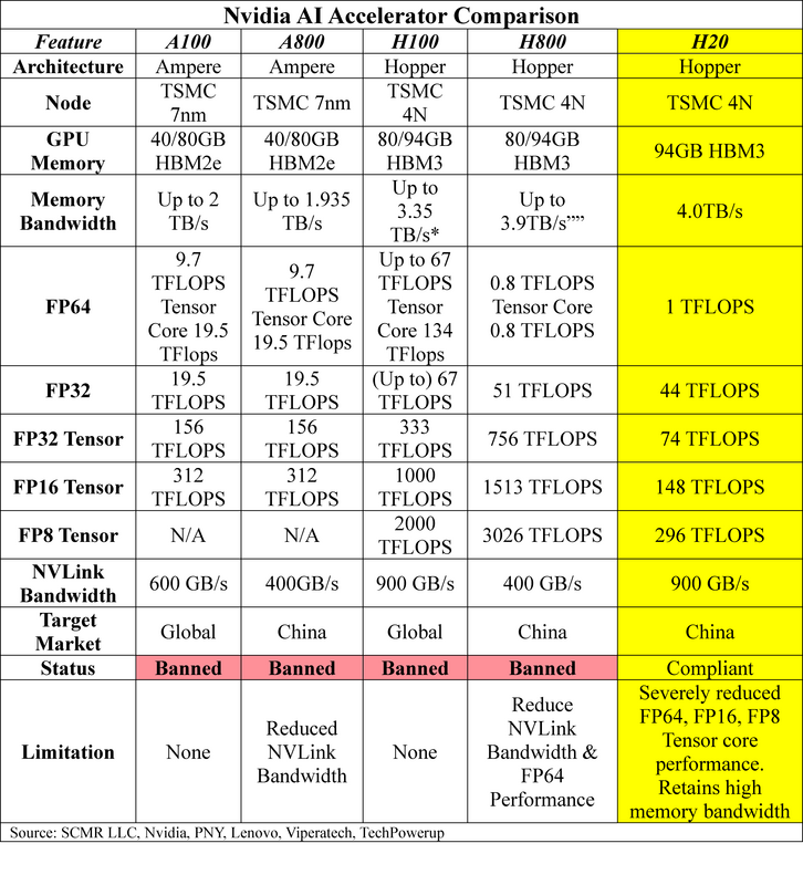
To understand the Nvidia H20 processor's capabilities compared to the currently banned AI chips, here's a detailed comparison table. More importantly, we break down what these technical metrics mean for AI and high-performance computing
[1] Note that the Nx or Xnm designations do not always correspond to actual sizes. N4 is actually part of the N5 ‘family’.
To understand the Nvidia H20 processor's capabilities compared to the currently banned AI chips, here's a detailed comparison table. More importantly, we break down what these technical metrics mean for AI and high-performance computing
- Architecture – Newer is typically better for GPU performance. Blackwell architecture is Nvidia’s latest innovation but is currently banned for export to China. A ‘de-featured’ Blackwell GPU for China is expected from Nvidia. That product should fall below government-mandated AI chip performance limits. Hopper architecture was announced in 2022, while Ampere architecture was announced in 2020.
- Node – A lower designation typically indicates a more advanced manufacturing process. TSMC’s N7[1] process was released in 2018 and uses DUV (Deep Ultraviolet) lithography.. It generated a 35% - 40% improvement in speed or 65% lower power consumption vs. 16nm process node. TSMC’s N4 process was released in 2022 and uses EUV (Extreme Ultraviolet Lithography). Versus the N5, the N4 showed an 11% performance boost, 22% higher power efficiency, and 6% higher transistor density.
- GPU Memory – Higher memory capacity and speed are crucial for AI workloads. HBM (High Bandwidth Memory) was released in late 2019 and supports 8 DRAM stacked dies. It runs (up to) a 3.6Gbps per pin data rate, with each stack having a 460GB/s bandwidth. The HBM3 (2022) supports a 12 stack architecture. It has (up to) a 6.4Gbps per pin data rate, with the latest HBM3e extending that to 9.6Gbps, so a nearly double data rate from the previous version.
- Memory Bandwidth – More is better for data intensive tasks.
- FPxx – These represent data types (Floating Point) and various precision levels. FP64 (Double Precision) is the highest precision level, while FP16 (Half Precision) is less precise but consumes much less memory and compute resources, making it the choice for deep learning tasks. For all, higher TFLOPS (Tera Floating Point Operations per Second) means higher performancer but tradeoffs are sometimes necessary to manage costs. We note that both Nvidia GPUs feature CUDA (General Purpose) cores and Tensor (Multi-matrix) cores and are available in these processors. We show performance for both.
- NVLink – This is Nvidia’s proprietary high-speed interconnect that is used between GPUs. It provides a higher bandwidth and lower latency that PCle. It also allows Nvidia GPUs to directly access each other’s memory allowing it to be ‘pooled’ rather than individually managed.
- Target Market – The initial market the GPU was designed for.
- Current Ex/Im status – The current export/import status under US regulations.
- Limitations – Some details on how formerly compliant devices met rules.
[1] Note that the Nx or Xnm designations do not always correspond to actual sizes. N4 is actually part of the N5 ‘family’.
Overall, if the US government follows through on granting a license for the Nvidia H20, it will put Nvidia back on the boards in the China AI chip market, perhaps reversing much or all of the $4.5b H20 inventory write-down that the company took in fiscal 1Q, in the form of even higher profit margins. We doubt they will have any trouble selling the inventory as Chinese buyers are already lining up for these newly compliant processors, but the question remains as to why the administration decided to allow this ‘give’ to China. Most likely it was a necessary ‘gift’ to encourage movement during the current trade negotiations, but one that goes against the concept of limiting China’s access to processors that could be used to advance the Chinese military. But while most would not feel that Nvidia has been treated unfairly considering they hold the premier global position in the AI GPU race, they have been severely limited when selling into the world’s largest market, so it seems about time that the company caught a break.
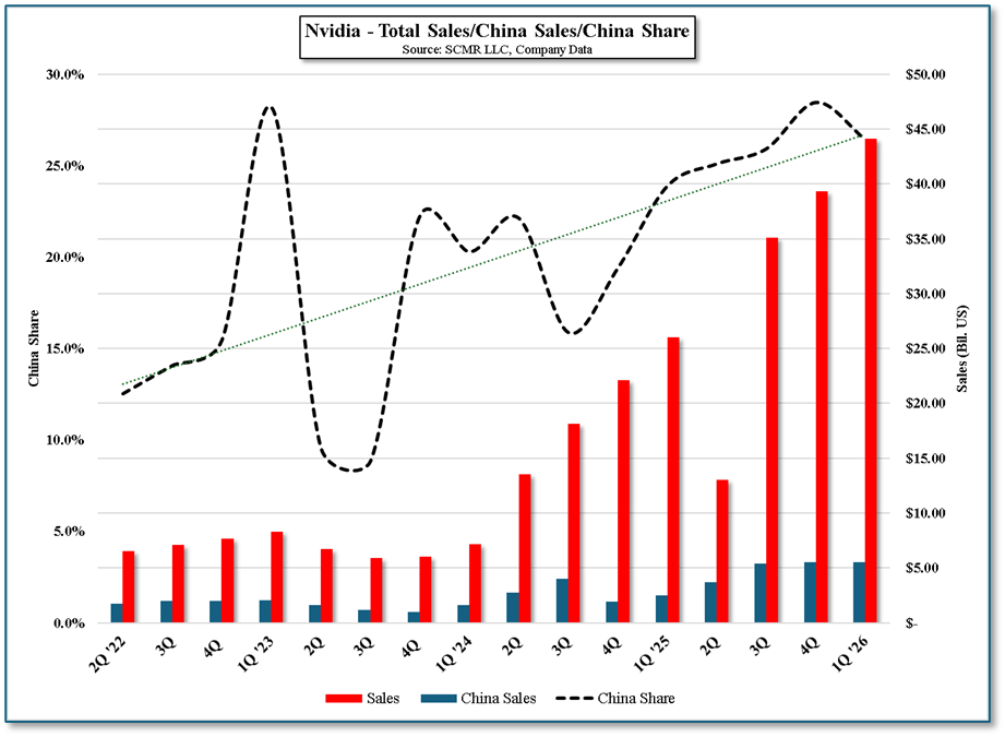
Figure 1 - Nvidia - Total Sales/China Sales/China Share - Source: SCMR LLC, Company Data
 RSS Feed