The Path to Brighter Displays – The “More Stuff” Strategy
There are two kinds of displays. Those that use a light source to illuminate colored materials and those that generate the colored light themselves (self-emitting). Material scientists are constantly working toward improving these materials, particularly the self-emitting group (OLED and quantum dots) as they must compete directly with non-self-emissive materials used in LCD (Liquid Crystal Display) devices, typically based on LEDs which are known for their brightness. However the pace of material science improvements does not lend itself to the more aggressive competitive pace of the consumer electronics industry and material scientists and display engineers find themselves looking for ways to improve self-emitting display performance more quickly.
Anatomy of the OLED Stack: A Microscopic Viral Frontier
Back roughly 15 years ago the ‘stack’ of OLED materials that was used to generate images consisted of two factions.
Small Displays – These devices, primarily smartphones, were built on an OLED stack consisting of a red phosphorescent material, a green fluorescent material (later this changed to phosphorescent material) and a blue fluorescent material, accompanied by a number of other ‘helper’ materials, along with an anode and a cathode. Each pixel contained the same structure. This was the typical configuration for small displays, primarily smartphones and tablets. These displays were produced in a vacuum chamber where the materials are sublimated (heated, turning them from a solid to a gas with no liquid state) and flow onto the substrate (typically glass or polyimide (plastic) on glass, with the glass later removed. This deposition of materials is done through a metal mask (think very fine screen) that creates the dots of material that become pixels on the screen.
Figure 1 - RGB Patterning - Source: Slashgear.com
Large Displays – As the metal masks used in small displays were not able to scale up in size (they sag), LG Display (LPL) developed an alternative. They coated the entire substrate with a blue fluorescent and a yellow/green phosphorescent material. When activated this produces a white light. That light passed through a color filter, a sheet of very small red green and blue phosphor dots, which create the colors you saw on the screen.
Figure 2 OLED with Color Filter - Source: SCMR-LLC
Over the years pixel layouts, materials, and processes changed and improved, but the basics remained the same until 2021 when Samsung Display (pvt) announced that it had developed a commercial large panel OLED display using both OLED materials and quantum dots. Quantum dots are molecules that can exchange the ‘color’ of light for another color. In Samsung’s case blue OLED material produced light that was converted into red and green light (clear space for blue) and a 3rd OLED process became available.
Understanding the Materials
The average display user knows little about the inner workings of displays, and in many cases investors only look at large scale production and shipment volumes to gauge the status of the industry, but behind those numbers are some details that can give indications as to more subtle trends that can become significant over time. In order to understand that nuance, one needs a more detailed understanding of the materials in an OLED stack
The stack in an OLED display is made up of a number of materials, each with a specific function:
Cathode – Typically a Magnesium/Silver or Aluminum alloy. In top emitting OLEDs the cathode is transparent and is between 10nm and 20nm thick. In bottom emitting OLEDs the cathode can be up to 100nm thick. This is one side of the electrical connection that causes the OLED materials to emit light (the negative side).
Electron Injection Layer – Typically Lithium Fluoride or Ytterbium between 0.5nm and 2nm thick. Acts as a ‘door’ to help electrons jump from the cathode to the next layer.
Electron Transport Layer – Typically an organometallic aluminum compound[1], roughly 20 nm to 40 nm thick. Essentially a highway for electrons.
Emissive Layer – Materials in this layer, either fluorescent or phosphorescent, are the ones that create the ‘glow’ of the display. Depending on the material, this layer is between 20nm and 40nm.
Hole Transport Layer – Typically TAPC[2] roughly 20nm to 60nm thick. A highway for holes (positive charge)
Hole Injection Layer – Typically HAT-CN[3] - That same ‘door’ for holes
Anode – Typically Indium Tin Oxide (ITO) or silver, between 50 and 100nm thick
This means that those little ‘glowy’ things on your TV or phone are roughly the thickness of a Flu virus, with each performing a task that enables the emissive material to produce as much light as possible.
Note: sometimes OLED display producers put ‘barrier or blocking layers on either side of the emitting material to make sure electrons and holes don’t overshoot their marks.
The "Cubed" Constraint: Why Thicker Isn't Always Brighter
Since all of these materials work toward making emitters produce light, as electrons and holes meet in the center of the stack, why not just add more materials to make OLED displays brighter? There are some specific reasons:
As competitive LCD displays are known for their brightness, OLED material scientists sought a way to close the brightness gap. Faced with the inability to gain brightness by using thicker emitter material, they came up with a ‘tandem’ solution. Instead of thickening the EML (Emitter Layer) they improved the architecture with a special layer, called a charge generation layer (CGL), between two thin emitting layers. The CGL acts as a relay station, allowing electrons passing through the 1st EML to ‘retire’, while creating new electrons for the second EML layer. This trick keeps electrons from building up and clogging the system.
There is a cost in terms of higher voltage needed for the two layers and the CGL itself, but the current remains the same as in a single layer and that keeps them from being destroyed. While the higher voltage is a ‘cost’, it is far less than the ‘cubed’ voltage of using a single thicker EML. As the EML/CGL layers are wired in series, a single stack that used 4 volts would need 8 volts for a tandem device, 12 volts for 3 layers, and so on, but the current stays the same, and current is the actual killer of the OLED material. Samsung has latched on to tandem technology and is now able to claim vastly improved device specifications under this architecture.
[1] Tris(8-hydroxyquinolinato)aluminium or Tris(8-hydroxyquinoline)aluminum.
[2] 1,1-Bis[(di-4-tolylamino)phenyl]cyclohexane
[3] Hexaazatriphenylenehexacarbonitrile
Understanding the Materials
The average display user knows little about the inner workings of displays, and in many cases investors only look at large scale production and shipment volumes to gauge the status of the industry, but behind those numbers are some details that can give indications as to more subtle trends that can become significant over time. In order to understand that nuance, one needs a more detailed understanding of the materials in an OLED stack
The stack in an OLED display is made up of a number of materials, each with a specific function:
Cathode – Typically a Magnesium/Silver or Aluminum alloy. In top emitting OLEDs the cathode is transparent and is between 10nm and 20nm thick. In bottom emitting OLEDs the cathode can be up to 100nm thick. This is one side of the electrical connection that causes the OLED materials to emit light (the negative side).
Electron Injection Layer – Typically Lithium Fluoride or Ytterbium between 0.5nm and 2nm thick. Acts as a ‘door’ to help electrons jump from the cathode to the next layer.
Electron Transport Layer – Typically an organometallic aluminum compound[1], roughly 20 nm to 40 nm thick. Essentially a highway for electrons.
Emissive Layer – Materials in this layer, either fluorescent or phosphorescent, are the ones that create the ‘glow’ of the display. Depending on the material, this layer is between 20nm and 40nm.
Hole Transport Layer – Typically TAPC[2] roughly 20nm to 60nm thick. A highway for holes (positive charge)
Hole Injection Layer – Typically HAT-CN[3] - That same ‘door’ for holes
Anode – Typically Indium Tin Oxide (ITO) or silver, between 50 and 100nm thick
This means that those little ‘glowy’ things on your TV or phone are roughly the thickness of a Flu virus, with each performing a task that enables the emissive material to produce as much light as possible.
Note: sometimes OLED display producers put ‘barrier or blocking layers on either side of the emitting material to make sure electrons and holes don’t overshoot their marks.
The "Cubed" Constraint: Why Thicker Isn't Always Brighter
Since all of these materials work toward making emitters produce light, as electrons and holes meet in the center of the stack, why not just add more materials to make OLED displays brighter? There are some specific reasons:
- Organic (OLED) materials are sensitive to degradation, but that degradation is not linear. A particular law of physics shows that the current density, the voltage and the material thickness are interrelated using the following formula with L3 being the thickness cubed. Therefore, as the thickness is the denominator, a small increase in thickness requires a very large increase in voltage, essentially doubling the thickness increases the necessary voltage by 2.8 times (constant current). which would crystalize the organic material. If we leave the voltage the same while doubling the thickness, the current falls below the point where the OLED would turn on..
- Additionally, as the thickness increases, the electrons and holes have difficulty getting through the material and pile up as they enter the emitter material. This requires even more voltage to push them through, so if the heat from the increased voltage didn’t degrade the material, the additional heat needed to push them through at this point would.
As competitive LCD displays are known for their brightness, OLED material scientists sought a way to close the brightness gap. Faced with the inability to gain brightness by using thicker emitter material, they came up with a ‘tandem’ solution. Instead of thickening the EML (Emitter Layer) they improved the architecture with a special layer, called a charge generation layer (CGL), between two thin emitting layers. The CGL acts as a relay station, allowing electrons passing through the 1st EML to ‘retire’, while creating new electrons for the second EML layer. This trick keeps electrons from building up and clogging the system.
There is a cost in terms of higher voltage needed for the two layers and the CGL itself, but the current remains the same as in a single layer and that keeps them from being destroyed. While the higher voltage is a ‘cost’, it is far less than the ‘cubed’ voltage of using a single thicker EML. As the EML/CGL layers are wired in series, a single stack that used 4 volts would need 8 volts for a tandem device, 12 volts for 3 layers, and so on, but the current stays the same, and current is the actual killer of the OLED material. Samsung has latched on to tandem technology and is now able to claim vastly improved device specifications under this architecture.
[1] Tris(8-hydroxyquinolinato)aluminium or Tris(8-hydroxyquinoline)aluminum.
[2] 1,1-Bis[(di-4-tolylamino)phenyl]cyclohexane
[3] Hexaazatriphenylenehexacarbonitrile
Figure 3 - Typical RGB OLED Stack - Source: SCMR-LLC
The Tandem Solution: The Efficiency Relay Station
Using the tandem theory, it would make sense for OLED display producers to keep adding additional layers, which, in theory, would produce brighter OLED display. Of course there are tradeoffs; the cost of the additional materials, the cost of processing the extra layers, the light loss from the additional layers[1], the lower yield (more layers more chance of issues and higher cost of ‘bad’ stacks), and more difficulty keeping the stack cool. However keeping those tradeoffs under control has been the goal of OLED display producers, and while they are primarily used in high-end devices where the BOM is a bit more flexible, the goal is for bringing tandem OLED to lower-priced devices. Apple (AAPL) has used tandem displays for the iPad Pro, Huawei (pvt) has used them for their high-end smartphones, as has Honor (pvt), while OLED display producers Samsung Display , LG Display, BOE (200725.CH), Visionox (002387.CH), and Tianma (000050.CH) all produce various tandem displays.
LG Display, the producer of WOLED large panel displays also uses a form of tandem display stack for their high-end OLED TVs. LG’s typical OLED stack (Figure 4) consisted of a blue fluorescent emitter, a yellow/green phosphorescent emitter, and a second blue fluorescent emitter. that when combined produced a white light. However, In order to maintain ‘high’ brightness, LGD added an additional sub-pixel that allowed the white light to also shine through as a 4th ‘color’ (RGBW) While this improved brightness, it also washed out some of the overall display color. They have since pushed that stack to higher levels by changing the yellow/green layer to separate red and green layers, which they say increased brightness by 33% and no longer have to rely as much on the white pixel, which they have removed on some models.
[1] While the layers ate thin enough to look clear, each layer reduces the total light passing through the stack by a small amount.
Figure 4 - Typical LF Display WOLED Stack - Source: SCMR-LLC
Figure 5 - LG Display's Tandem OLED Stack - Source: SCMR- LLC
The "Penta Tandem" Push: Samsung’s Structural Brute Force
Unusually , while Samsung Display produces tandem displays for clients, particularly Apple, they do not use tandem RGB technology in their own products. Some (particularly Samsung) say that this is because Samsung’s displays are already equal to or more efficient than tandem displays, while others say it is just a matter of cost and time before they adopt the technology. They do use a form of tandem technology for their IT and TV products where they take the technology to what might be called an extreme, as noted below.
Samsungs original QD/OLED stack was already a quad OLED stack when it was first released in 2021. Their first QD/OLED display (2021) was the quad stack you see below in Figure 6, which has remained the company’s QD/OLED stack since. However they have been using a Penta-Stack architecture, that incorporates an additional blue and Charge Generation layer on some of their high-end (S95F) models since last year. As of this month Samsung Display has officially trademarked the “Penta Tandem” brand and will be using this architecture for all 27” (new), 31.5”, and 49” monitors. The Samsung S95 series, Samsung’s top-of-the-line QD/OLED TVs, along with Sony’s (SNE) top level QD/OLED TVs (Bravia 8 III) will have the Penta stack while lower tier models will still use the quad architecture,.
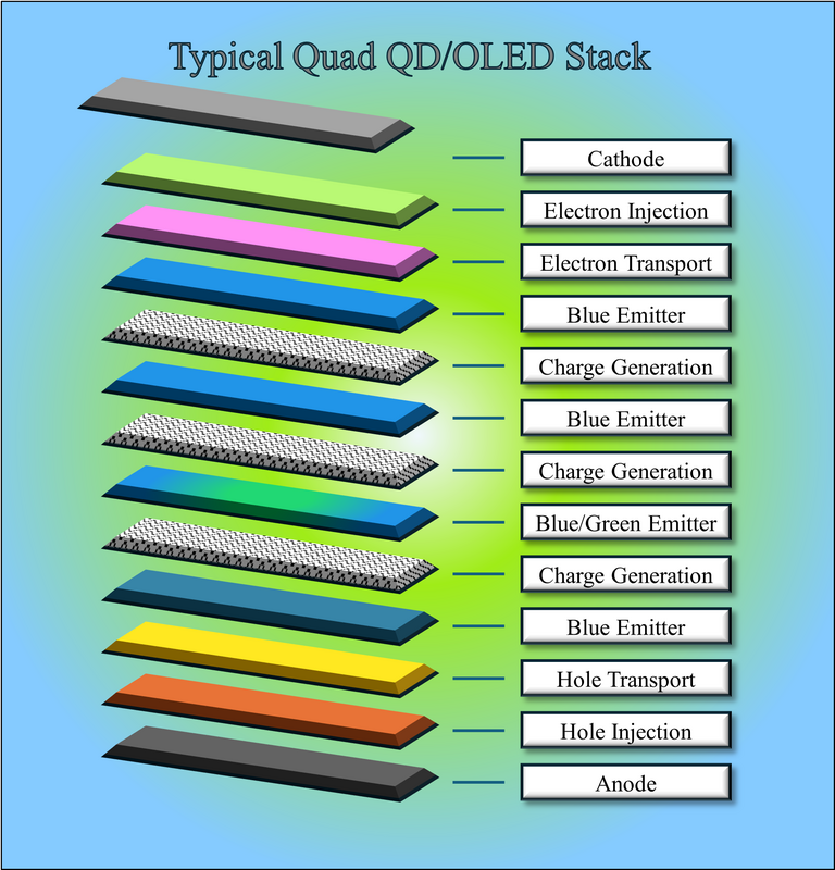
Figure 6 - Typical Quad QD/OLED Stack - Source: SCMR-LLC
The UDC Connection: The Phosphorescent Blue "Holy Grail"
The comparison between these OLED stacks seems quite esoteric to most, but in fact, it is of utmost importance to investors who are involved in a number of companies, particularly Universal Display (OLED), the supplier of red and green phosphorescent material to the industry. UDC typically supplies these materials under two contracts.
Phosphorescent materials differ from fluorescent materials in that they are1 relatively slow to convert energy into light and blue phosphorescent materials are the slowest. They are so slow (relative term) that they tend to bump into each other and annihilate themselves, producing heat and energy but no light, doing further destruction to the source materials. As phosphorescent materials are ‘doped’ into a host material, the host material must be able to withstand even higher energy levels than the blue material itself and there are few host materials that have this capability. All of these issues have made it extremely hard to find a blue phosphorescent emitter that is efficient, has a deep color, and has a commercially viable lifetime. Material scientists can play with these three metrics, but they affect each other, Pushing one tends to reduce another so the balance between them is the key to success.
In lieu of a blue phosphorescent, OLED producers use blue fluorescent emitters which are far less efficient but have a longer lifetime and are relatively inexpensive. OLED systems like Samsung’s Penta QD/OLED use multiple layers of blue fluorescent material to compensate for its lower efficiency, while UDC and other s are hoping that a new blue phosphorescent material can replace all of those blue fluorescent layers with one phosphorescent blue layer.
The Pricing Paradox: Material Cost vs. Structural Complexity
As Samsung Display does not have a license to use a blue phosphorescent emitter, should UDC release one, they will have to negotiate separate material supply and license contracts. We expect the blue material, when commercialized will be the most expensive of the three (RGB) and will be priced at a significant premium to blue fluorescent material. In order to understand that pricing one must look at the cost of multiple blue fluorescent layers and the CGLs needed to make them efficient enough to match a blue phosphorescent material, at which point the premium pricing become more obvious. If it takes four or five fluorescent blue layers to produce the same metrics as a blue phosphorescent layer, logically UDC will assess the fluorescent stack costs and price the blue phosphorescent at an equivalent level or above (the convenience factor), but that would be a wash for Samsung who could then choose to stay with its ‘Penta’ (five blue fluorescent layer) architecture. This would be a serious loss for UDC who counts SDC as one of its top customers. We expect a more realistic starting price of 7 to 10 times the average price of green phosphorescent emitter material, rather than the ~20 times that a ‘Penta’ equivalent might reflect.
So, our expectations are that if and when UDC announces a commercial blue phosphorescent stack system they will price the material much lower than Samsung’s equivalent ‘Penta’ cost, not as low as red or green, but not the massive step up that a penta-equivalent might foretell. That might get the negotiations through the material contract but there is also the license. We believe Samsung pays ~75% in license fees for every $1.00 it purchases in red and green materials and they will have to negotiate a license agreement with UDC for blue. Looking at that same 75% rate on top of the higher cost of the blue material, Samsung would be paying quite a bit more to UDC to use their full color stack, making their ‘Penta’ alternative a more attractive possibility..
Investor Outlook: Samsung’s Strategic Stalemate
Samsung Display has given itself the option to stick with its Penta (or more) layer system if UDC pushes for an excessive premium blue phosphorescent material and license price. If they are able to match the specs of UDC’s blue phosphorescent material they can hold off an agreement until the price of blue comes down or lower cost volume agreements can be reached. It might be a more difficult marketing approach for Samsung, but they are known as a very aggressive negotiator. In this case they are not left without an alternative. The idea of a ‘Penta’ brand sets up Samsung’s bargaining position and gives the company an alternative if negotiations become difficult. We expect preliminary talks between the two have been ongoing, but once blue is officially commercialized, the real negotiations begin.
UDC - Thursday (Feb 19th) Earnings Call
Universal Display will release 4Q results on Thursday and will possibly give guidance for 2026. That guidance will be an indicator as to the confidence level UDC has in both the commercial release of a phosphorescent blue stack, their ability to negotiate material supply contracts with their customers, and their confidence level concerning a definitive agreement with Samsung Display. Of course, they can always pass on giving guidance or change it if necessary but guidance for a strong year could indicate the inclusion of blue.
Conclusion: The Tandem Trap and the Blue Grail
The evolution from the single-stack architectures of 2011 to Samsung Display’s 2026 "Penta Tandem" branding marks a pivotal shift in the display industry’s power dynamics. By moving to a five-layer structure, Samsung has essentially engineered its way around the "Blue Efficiency Gap." They are using volume and architecture to compensate for material limitations, a "brute force" method that is both a marvel of manufacturing and a strategic defensive wall against high material costs.
For Universal Display (UDC), the stakes for Thursday’s call are binary:
The comparison between these OLED stacks seems quite esoteric to most, but in fact, it is of utmost importance to investors who are involved in a number of companies, particularly Universal Display (OLED), the supplier of red and green phosphorescent material to the industry. UDC typically supplies these materials under two contracts.
- Material supply contracts that set loose volume requirements and discount volume trigger points. We say loose as UDC has been known to relax full year volume contractual obligations (usually pushing the unused portion into the coming year). This flexibility helps UDC maintain reasonable relationships with all OLED producers across the industry. We believe all but one of UDC’s material supply contracts cover the full range of UDC materials, including a phosphorescent blue emitter under development. Samsung Display is the exception as their material supply contract covers only red and green emissive materials.
- License/Royalty contract - The second contract is a more complex one involving UDC’s ownership of the right to use organo-metallic phosphorescent OLED materials in a device. All but one of UDC customers pay a per unit royalty based on factory level device pricing, although the recognition of that revenue is tied to material sales under ASC 606. The one exception is Samsung Display who pays a quarterly flat license fee and no unit royalty.
- Improve internal material efficiency by 4x
- Reduce power consumption by 25% to 30%
- Reduce heat issues
- Allow for smaller pixels/higher resolution
- Improve blue lifetime
Phosphorescent materials differ from fluorescent materials in that they are1 relatively slow to convert energy into light and blue phosphorescent materials are the slowest. They are so slow (relative term) that they tend to bump into each other and annihilate themselves, producing heat and energy but no light, doing further destruction to the source materials. As phosphorescent materials are ‘doped’ into a host material, the host material must be able to withstand even higher energy levels than the blue material itself and there are few host materials that have this capability. All of these issues have made it extremely hard to find a blue phosphorescent emitter that is efficient, has a deep color, and has a commercially viable lifetime. Material scientists can play with these three metrics, but they affect each other, Pushing one tends to reduce another so the balance between them is the key to success.
In lieu of a blue phosphorescent, OLED producers use blue fluorescent emitters which are far less efficient but have a longer lifetime and are relatively inexpensive. OLED systems like Samsung’s Penta QD/OLED use multiple layers of blue fluorescent material to compensate for its lower efficiency, while UDC and other s are hoping that a new blue phosphorescent material can replace all of those blue fluorescent layers with one phosphorescent blue layer.
The Pricing Paradox: Material Cost vs. Structural Complexity
As Samsung Display does not have a license to use a blue phosphorescent emitter, should UDC release one, they will have to negotiate separate material supply and license contracts. We expect the blue material, when commercialized will be the most expensive of the three (RGB) and will be priced at a significant premium to blue fluorescent material. In order to understand that pricing one must look at the cost of multiple blue fluorescent layers and the CGLs needed to make them efficient enough to match a blue phosphorescent material, at which point the premium pricing become more obvious. If it takes four or five fluorescent blue layers to produce the same metrics as a blue phosphorescent layer, logically UDC will assess the fluorescent stack costs and price the blue phosphorescent at an equivalent level or above (the convenience factor), but that would be a wash for Samsung who could then choose to stay with its ‘Penta’ (five blue fluorescent layer) architecture. This would be a serious loss for UDC who counts SDC as one of its top customers. We expect a more realistic starting price of 7 to 10 times the average price of green phosphorescent emitter material, rather than the ~20 times that a ‘Penta’ equivalent might reflect.
So, our expectations are that if and when UDC announces a commercial blue phosphorescent stack system they will price the material much lower than Samsung’s equivalent ‘Penta’ cost, not as low as red or green, but not the massive step up that a penta-equivalent might foretell. That might get the negotiations through the material contract but there is also the license. We believe Samsung pays ~75% in license fees for every $1.00 it purchases in red and green materials and they will have to negotiate a license agreement with UDC for blue. Looking at that same 75% rate on top of the higher cost of the blue material, Samsung would be paying quite a bit more to UDC to use their full color stack, making their ‘Penta’ alternative a more attractive possibility..
Investor Outlook: Samsung’s Strategic Stalemate
Samsung Display has given itself the option to stick with its Penta (or more) layer system if UDC pushes for an excessive premium blue phosphorescent material and license price. If they are able to match the specs of UDC’s blue phosphorescent material they can hold off an agreement until the price of blue comes down or lower cost volume agreements can be reached. It might be a more difficult marketing approach for Samsung, but they are known as a very aggressive negotiator. In this case they are not left without an alternative. The idea of a ‘Penta’ brand sets up Samsung’s bargaining position and gives the company an alternative if negotiations become difficult. We expect preliminary talks between the two have been ongoing, but once blue is officially commercialized, the real negotiations begin.
UDC - Thursday (Feb 19th) Earnings Call
Universal Display will release 4Q results on Thursday and will possibly give guidance for 2026. That guidance will be an indicator as to the confidence level UDC has in both the commercial release of a phosphorescent blue stack, their ability to negotiate material supply contracts with their customers, and their confidence level concerning a definitive agreement with Samsung Display. Of course, they can always pass on giving guidance or change it if necessary but guidance for a strong year could indicate the inclusion of blue.
Conclusion: The Tandem Trap and the Blue Grail
The evolution from the single-stack architectures of 2011 to Samsung Display’s 2026 "Penta Tandem" branding marks a pivotal shift in the display industry’s power dynamics. By moving to a five-layer structure, Samsung has essentially engineered its way around the "Blue Efficiency Gap." They are using volume and architecture to compensate for material limitations, a "brute force" method that is both a marvel of manufacturing and a strategic defensive wall against high material costs.
For Universal Display (UDC), the stakes for Thursday’s call are binary:
- The Revenue Ceiling: If UDC prices their upcoming Blue Phosphorescent emitter too close to the "Penta-equivalent" cost (~20x green), they risk Samsung simply staying with their established, trademarked five-layer fluorescent system. To win, UDC must price Blue low enough to offer a genuine BOM reduction, not just a performance wash.
- The Samsung Stalemate: The fact that Samsung’s current contract excludes blue while they aggressively trademark "Penta Tandem" as an alternative suggests they are prepared to negotiate from a position of strength. They have proven they can achieve 4,500 nits and double lifespans using "inferior" fluorescent materials; they do not need UDC’s blue at any price or at least present that image.
- Guidance as a Tell: If UDC guides for a record 2026 (Consensus: $700M+), they are signaling that a deal with Samsung or a broad commercial launch is imminent. If the guidance is conservative, it implies the "Penta Tandem" vs. "PHOLED Blue" standoff continues. No guidance puts the entire question back another quarter and indicates either the material is still not ready for commercial production or negotiations with key customers are still in progress.
 RSS Feed