Supply Chain Market Research - SCMR LLC
  • Blog
  • Home
  • About us
  • Contact

Chinastar Pulls In New Fab Plans

8/5/2021

0 Comments


Chinastar Pulls In New Fab Plans
​

​Chinastar (pvt), a subsidiary of parent TCL (000100.CH) has indicated that it expects its latest LCD fab project, T9 to achieve mass production earlier than expected.  The original plan for the fab was to begin mass production in early 2023, which the COO now believes will take place before the end of 2022, a pull in of at least three months based on their schedule.  The new fab has a planned capacity of 120,000 sheets/month using a 2250 x 2600 sheet format (Gen 8.5) and has been designed to produce IT products using an IGZO backplane, a technology that Chinastar has considerable experience with.
While we had originally modeled April 2023 at the start date for the fab, we had planned for only relatively small production until July ’23.  With the expected pull-in, we move the start date to October 2022 and a serious ramp beginning in January 2023. , and additional lines scheduled in 2023 and 2024.  While pull-ins and push-outs are fairly common in the display space, we expect the optimistic view that panel producers have developed over the last year, a result of the rapid increase in large panel prices, will push timelines on new capacity projects further.  While large panel prices may flatten and even decline, most panel producers remain in a profitable position, and the mindset does not change easily when profits are accumulating.
That said, big capacity projects like T9 can have a significant impact on the supply/demand curve and as such projects enter production overall production utilization can take a hit.  If the IT panel market shows any signs of a real demand slowdown, and not one caused by shortages or the end of a shortage cycle, it will take some time before panel producers are willing to change their capacity increase schedules, and the industry could easily settle back into its more typical boom/bust pattern.  Many panel producers believe its different this time due to COVID-19, which we admit has been true, but human nature is such that it reverts back to norms as soon as possible.  Whether that is later this year or next will impact those decisions but not until it is likely too late to make substantial changes.  Alea iacta est – loosely translated, passed the point of no return…
0 Comments

Micro-LED Forecast, But…

8/4/2021

0 Comments


Micro-LED Forecast, But…
​

​Forecasting new and early developing technology is like herding cats, they never seem to wind up where they were supposed to be, but despite the vast number of technical, process and potential unknowns, the folks at Trendforce are trying their hand at predicting the future for Micro-LEDs.  As Trendforce is based in Taiwan, and Taiwan is the locus for much of the LED industry, it makes sense that if anyone would want to wax optimistic about micro-LEDs it would Taiwanese analysts.  While they do not give much of their absolute data to us mere mortals, they do predict that annual revenue from Micro-LED Chips used in TV applications will be ~23m this year, growing slowly in 2022 (we ballpark at $50 -75m), a bit faster in 2023 (~$350m) and 2024 (~$900m), but spiking to $3.44b in 2025.
While the details are sparse, they do cite a number of challenges that need to be met in order to reach these goals, with the cost of the micro-LED chips themselves the biggest stumbling block, a logical conclusion given the almost 25m needed for a 4K TV and the necessity for almost absolute uniformity across such vast numbers, something the industry is unable to do presently.  As we have mentioned a number of times, the transfer process for such large numbers and such small devices, is also a major challenge, one that has spawned a number of competitive solutions that have yet to prove themselves effective, but they did mention one area in the development of micro-LEDs that tends to be overlooked, and that is testing. 
Standard practice for testing LEDs is photoluminescence, which allows larger LEDs to be ‘binned’ (classified) by their brightness, so systems such as LED backlights have uniformity.  However when LEDs drop to the sizes that will be needed for micro-LED displays that are within normal parameters (say 65” or 75”), it gets progressively harder to make those measurements and obviously more time consuming based on the number of micro-LEDs.  Without a repeatable and consistent ability to test micro-LEDs, particularly before they are transferred to a substrate, the technology will be unable to compete and the transfer process will become moot, so with open questions as to just these few challenges to the development of Micro-LEDs we see forecasts as laced with too many …but, if...’s to be of service.  Maybe it sells expensive reports, but while we commend those who can see into the future, we would rather see continuing updates on the progress of the challenges mentioned and those that will potentially appear when the first set are solved than forecasts that we know will have little relevance to actual commercial development and implementation. 
0 Comments

Dot Dash

8/4/2021

0 Comments


Dot Dash
​

Quantum Dots have been around for many years, but right around the time that commercial OLED TVs were being shown at CES for the first time, quantum dot films began to appear in the vocabulary of display manufacturers.  These semiconductor crystals, which vary in size from 2um to 10um, have the unique property of being able to convert light of one color (frequency) into another, with that ability being determined by the QD size, with the larger dots converting to red, intermediate size converting to green, and the smallest sizes converting to blue. 
This means by ‘tuning’ the size of the QD crystals when they are synthesized, they can be used to convert light of a particular frequency (color) to another color.  This differs from phosphors, which typically ‘block’ the light of other colors, with a red phosphor removing the blue and green from a white light and letting only the red light pass.  Phosphors therefore reduce the light energy output significantly, while quantum dots ‘shift’ the energy rather than reduce it.
Quantum dots also have other beneficial characteristics, particularly their ‘narrow’ output relative to other materials, which gives them the ability to generate ‘pure’ colors that allow displays to more precisely control the colors that are produced.  As quantum dots are ‘stimulated’ by light, they are ideal for QDEF (quantum dot enhancement films) or QDOG (quantum dot on glass) systems that are the basis for many high-end TVs sold today, and have applications where they can replace typical phosphor based color filters in large size LCD and OLED displays, or can be used to convert a single color backlight into an RGB display at a low cost.
But quantum dots have another characteristic that makes them valuable in the display space, and that is not only can they convert the frequency of light that stimulates the QDs, but by applying an electrical charge to the QDs, they can produce light on their own.  This self-emissive property is similar to the plasma displays of years ago, where a gas was electrically stimulated to produce a colored dot, or OLED materials that have the same basic property.
Producing quantum dots is a chemical process that must be carefully controlled but is certainly viable for mass production and the move away from cadmium-based quantum dots has reduced or eliminated any question of safety for consumers, with the dots being combined in films or deposited directly on light guides in TV displays.  But to use quantum dots effectively for more sophisticated applications, they face the same issues as OLED materials, that of patterning, or precisely placing the dots on the corresponding points in the TFT (thin film transistor) circuitry that controls them.  In a 4K display this means over 24m quantum dots have to be correctly placed and in an 8K display just under 100m dots ‘spots’ must align with the TFT electronics.
Small OLED displays are able to use FMM (fine metal masks) to precisely place OLED materials when creating and RGB display, but those masks do not scale to the sizes needed for large OLED TVs, which uses two OLED materials that are coated across the entire display to produce white light, which is then converted to the three primary colors by a color filter.  As noted above, the color filter is ‘subtractive’ and reduces the light output of the display, which makes it more difficult for large OLED displays to compete with large LCD displays which tend to be brighter, so the idea of using quantum dots as self-emitting materials would offer a solution to that problem only if the QDs can be patterned across such large displays.
Ink-jet printing is one way that has been tried for patterning self-emissive materials, both OLEDs and quantum dots, but IJP involves dissolving the materials in solvents so they can pass through the ink-jet heads.  This can affect the materials, requires ‘curing’ before adjacent materials are deposited, and can add variability to the ink-jet droplets themselves.  While IJP is certainly a developing technology that is already used to a degree in the display space, a simpler and less ‘invasive’ process would likely be necessary if self-emissive quantum dots were to surface as a viable commercial display process.
Much research is being conducted on moving quantum dots from ‘converters’ to emitters’, but we have noticed that a group of engineers at a TCL (000100.CH)/Chinastar (pvt) Innovation center have come up with a novel approach to patterning quantum dots that seems to hold promise as a potentially commercial process.  The concept uses a process called electrophoretic deposition, which moves particles that are charged to an oppositely charged electrode.  Quantum dots can be charged by attaching positive or negative ions to the bonds that attach to the QD core and placing an oppositely charged material in the solution will attract the dots to that material, but that only gets them there en masse.
The trick that these researchers came up with is to use photolithography to produce an electrode that is patterned, and will only attract QDs where the pattern exists, similar to the way photolithography is used to produce the circuitry that is the basis for the millions of transistors that appear on semiconductor devices.  In the same way, second and third electrode pattern can also be created that would only attract QDs to those locations when turned on, so by charging each electrode only when it is in the proper ‘color’ solution, a complete RGB QD pattern can be created on large substrates, with the thickness of the material controllable by varying the time and strength of the electrical field.  In some cases the QDs might be stacked, which would entail simpler patterning and the same three dip process and the process is not limited to rigid substrates opening up the process to flexible and 3D structures.  The process (in the lab) took less than a minute for each color with about 20mins drying time for each.
While we don’t often cite lab technology, given the difficulty in transferring much of this kind of work into scalable production, much of this process uses existing technology that is available to display producers or is already part of their process, so it does have some relevance to a working solution that could one day be profitable.  The characteristics of quantum dots, particularly their inorganic nature (core) and their color purity make them viable candidates for self-emissive displays and such a more practical process could legitimize the continuing R&D into the development of a realistic Self-emissive QD product timeline.[1]


[1] Zhao, Jinyang. “Large-Area Patterning of Full-Color Quantum Dot Arrays beyond 1000 Pixels per Inch by Selective Electrophoretic Deposition.” Nature Communications.
 
Picture
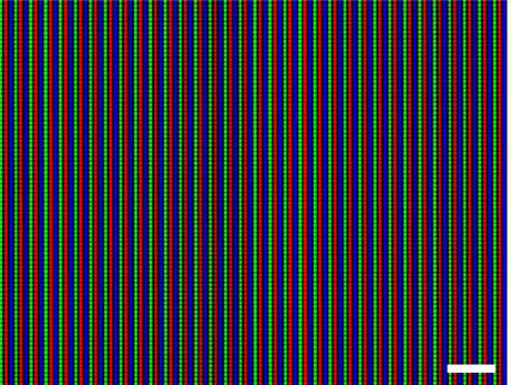
In-line Patterning Process on Electrode - Source: See Citation below
Picture
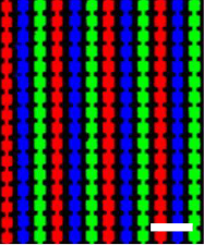
Fluorescent images of RGB QD patterns (3 Step) - Source: See Citation
Picture
0 Comments

Reducing the Noise

8/4/2021

0 Comments


Reducing the Noise
​

Headphones have been around for over 100 years but until John Kloss came up with the idea of stereo headphones in 1958 that were designed to actually listen to music most users were limited to headphones used in radio communication systems, and when the Sony (SNE) Walkman came out in 1979, the concept of earbuds became a worldwide phenomenon.  Over the last few years wireless headphones of all types have become the norm and the even more recent focus on ‘noise-cancelling’ headphones has given the headphone industry a needed shot in the arm, with the noise reduction on-line market growing by over 100% in 1Q of 2020, a particularly bad quarter for the entire industry.
Picture
Early Headphones - Source: Lstnsound.com
​TWS (true wireless stereo), at least at the high end, are usually equipped with noise-cancelling or noise-reduction systems, and that option is rapidly becoming a selling point for wireless headphones generally, with much of the promotion citing the lower volumes needed with noise-cancelling headphones, leading to less ear damage.  However the State Administration for Market Regulation in China conducted risk monitoring specifically for ‘active noise reduction headphones, including 60 models from 47 companies.
The results of the tests were a bit surprising in that 50% of the products checked were ‘insufficient in noise reduction’, which may cause consumers to increase the volume in noisy locations, which would increase the sound pressure level and result in hearing damage.  However that was less important than the fact that the etsts also concluded that 40% of the products that claimed to have noise reduction abilities, did not have support for any of those functions, with some having rudimentary technology and others none at all, despite the advertisements.
Since there is no uniform standard for what defines noise-reduction, on-line product promotion includes "active noise reduction", "hybrid noise reduction", "AI noise reduction", "deep noise reduction", "intelligent dynamic noise reduction", "hybrid digital noise reduction", "multi-dimensional noise reduction" and other equally nebulous wording and concepts that serve only to confuse consumers, and the inability of the technology in many of the tested products to perform even rudimentary noise reduction functions, such as balancing each ear.
Noise-reduction in such headphones is generated by external microphones (there should be one on each side) that sample the surrounding noise environment and generate an inverse audio image of the external noise, while leaving the music untouched.  This obviously entails a higher cost, not only of hardware, but also embedded R&D, either by chip manufacturers such as Mediatek (2454.TT), Qualcomm (QCOM), and Realtek (2379.TT), or in-house, and the cost of same can be enough that lower-cost TWS systems use generic chips rather than the company developed noise reduction processors, as Apple (AAPL) did with the Beats Studio BUD TWS.
The problem with noise reduction is that in many cases it eliminates things that are necessary for staying safe, such as the sound of a car approaching or the sound of a signal, and many of the algorithms have at least some effect on the overall quality of the music, but you can’t have it both ways, so while a good noise cancelling system might protect your ears in a noisy environment, they tend to give users a false sense of security as that crosstown bus bares down on your as you cross against the light.
The final outcome of the tests prompted the SAMR to issue a statement saying, “A large proportion of products have insufficient noise reduction control, and the accuracy of identifying external noise is also insufficient. At the same time, although the maximum sound pressure level index is relatively stable, consumers still need to pay attention to control the use time to avoid hearing damage,” which is a nice way of saying ‘buyer beware’.
0 Comments

Semiconductor Catch 22

8/3/2021

0 Comments


Semiconductor Catch 22
​

Semiconductor shortages have been a problem for the CE space for a year, with the situation worsening since the beginning of this year.  Semiconductor fabs are running at full capacity, and while conversations about fabs used to be centered around who would be producing at below 5nm, the focus these days is who has the most available capacity at 28nm and above, as these nodes are the workhorses of the semiconductor industry and produce much of what goes into most CE products.  Application processors for smartphones and similar products get quite a bit of attention as they lead the industry in transistor count and processing metrics, but things like display drivers, FPGAs, and lots of gut level silicon is what makes up most of the CE products we use on a daily basis, and many are really in short supply.
Building out semiconductor capacity takes lots of money and time, so a quick fix for the situation, despite the headlines, is not new fab construction as it will do little to change near-term capacity, and the capital investment cost of building smaller node fabs is easily twice that of building 28nm fabs, where the real capacity is needed.  With all semiconductor buyers competing for limited fab capacity and some of that fab capacity allocated to very specific products, prices continue to rise and while semiconductor foundries are making big plans for adding capacity, there is a Catch-22 that will slow those plans and extend the time it will take to bring that new capacity into the market.
Picture
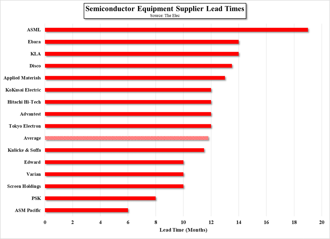
​Based on data accumulated by The Elec, semiconductor equipment suppliers are rapidly increasing the lead times for a wide variety of equipment, not because they cannot produce such tools, but because they do not have the semiconductors they need for the equipment and are on allocation at fabs along with the rest of the industry.  As was the case with automotive semiconductors, shortages caused serious ripples down the supply chain causing automotive assembly plants to be shuttered temporarily until governments began to pressure semiconductor foundries to allocate more capacity to the chips necessary to reopen those plants and put workers back on the lines.  Given that there were other products that produce higher returns for silicon producers, this took a bit of cajoling until a more reasonable balance was found.
Unfortunately, the same seems to be happening to semiconductor equipment suppliers who face shortages of the components they need to produce the semiconductor equipment that will eventually add enough capacity that we won’t have any semiconductor shortages, but such issues for tool vendors have extended equipment lead times by some extraordinary amounts, leading to an extension of the shortage cycle, a perfect Catch-22.   Demand has also contributed to the lead time issue, as semiconductor foundries have been stepping up orders for equipment as they face maxed out utilization rates and have to turn away business, but they do have the option to raise prices for what they are able to produce, which they have.  While equipment suppliers technically have the same option, higher prices make little difference if you cannot deliver product, so the supply chain slows and the crisis remains.
Based on the data we have seen (see below), average semiconductor equipment lead times have increased from between 3 to 6 months last year to ~10 months in the 1st quarter of this year and have continued to increase to between 11.3 months and 12.3 months on average, with some extending out as long as 24 months.  Based on the mid-point of those suppliers that gave a range, the average equipment lead time is 11.8 months, with both US and Japanese companies averaging 12.1 months and 12.2 months respectively.  ASM Pacific (522.HK), a supplier of dicing and bonding tools and Korea’s PSK (319660.KS), a supplier of dry stripping tools, being the lowest at 6 months and 8 months respectively, while ASML (ASML), Ebara (6361.JP), and KLA (KLAC) are the highest among those that were polled, at 19 months (average) and 14 months respectively, with the latter two the same.
Picture
Semiconductor Equipment Supplier Lead Times - Source: The Elec
0 Comments

Dark Mode – Does It Work?

8/3/2021

0 Comments


Dark Mode – Does It Work?
​

The CE space is ripe with claims; Claims that ‘my product’ is the best, or ‘we have the largest market share, or our product has the best technology, and as folks who look at and catalog massive amounts of data, we understand that making such claims by citing data is not always quite ethical, as narrowing data sets is a way to bring up standing, and the fine print at the bottom of the page that defines the data is rarely read.  That said, OLED displays have been making claims about how they save power when compared to LCD displays for many years and while the fine print is again a part of the answer to the validity question, from a logical standpoint, they should be less power hungry, at least for small panel OLED devices.
Small panel OLED displays use red and green phosphorescent OLED materials and a blue fluorescent OLED material to produce full color displays.  Since these materials are self-emitting, when a segment of the display is black, those pixels are turned off, reducing power consumption.  This differs from LCD displays, which generate light from an LED backlight, which passes through a liquid crystal ‘gate’ and on to a color filter that changes the white light to the three colors necessary to produce the millions of colors needed.  However, when a section of the image is dark, the liquid crystal gate closes, blocking the light to the user, but the backlight itself remains on, and continues to consume power, so from a technical perspective, an OLED display should consume less power.
But what about real life?  Does this really make that much of a difference to smartphones users, who would be the most affected by battery issues?  While LCD display users are typically looking at images displayed on a white background, OLED users have been told that the best way to use their OLED smartphones effectively is to switch to ‘dark mode’, where the background is black, but some users are not used to ‘dark mode’ and have resisted the change, and likely have compromised much of the power saving benefits of OLED displays.  This is particularly apparent with iPhone users, who have been exposed to OLED displays for only 4 years and less if you count the entire iPhone line, compared to Samsung users, who have been using phones with OLED screens since 2004.
There are some ground rules however before the question gets answered, as the brightness of the display, and by this we mean the user controlled brightness, has a great deal to do with the power consumption, regardless of the technology, so there is a material difference in results that would be generated in bright sunlight where the display would be turned up to full brightness as to those generated in relatively dark lighting situations.  The answer also does not consider the consequences of high brightness and low brightness on color correctness and the phone’s ability to correct for these circumstances, but the data does include a number of different models (model years) of the same phone, and a number of different applications to see if the application itself influences the results.  We show in the table below the averages to reduce the amount of data.
Picture
​When looking at the averages for all four OLED smartphones, the data confirms that ‘dark mode’ is a power saver at all three brightness levels.  In terms of the applications tested, one phone saw a 1% increase in power consumption at the lowest (30%) brightness level for three of the six applications tested.  Other than that all phones saw a reduction in power which ranged from 1% to 69%, by switching to dark mode, in all brightness modes, for all applications.  So with only the minor exceptions noted (this was from the oldest of the four phones) dark mode is a big benefit for those using OLED smartphones, and regardless of whether the OLED display inherently saves power over an LCD display at a variety of brightness levels, switching to dark mode will make sure you drain the least amount from your battery and have the longest time to use the phone between charges.  Thanks to Purdue students for conducting the very detailed analysis.
0 Comments

Samsung QD/OLED Project Update

8/2/2021

0 Comments


Samsung QD/OLED Project Update
​

While there has been considerable speculation about the status of Samsung Display’s (pvt) QD/OLED project and even more speculation about the technology being developed, on a general basis there were two paths for the development to take.  The first (simplified) is based on a substrate coated with a blue OLED emitting material and a color filter with quantum dot (red/green) converters.  In this mode the blue light generated from the OLED emitter, which is controlled by an active matrix TFT system similar to what is used in OLED TVs, reaches the color filter, which is configured as three sub-pixels in each pixel, all being individually controlled by the TFT.  In the case of two of the sub pixels, the blue light is converted into red and green, while the third sub-pixel is essentially a ‘clear’ window, allowing the blue light through.
This system differs in two ways from the approach that LG Display, the leading OLED TV panel supplier, uses for their TVs, which use two OLED layers (green/yellow and blue) that when combined generate white light.  That white light then passes to a color filter that uses red, green, and blue phosphors to filter out two of the three primary colors in white light to form red, green, and blue sub-pixels.  The important distinction here is that the ‘new’ QD/OLED process uses only one OLED color (blue), while the LGD process uses two and that the phosphors in the LGD color filter are ‘subtractive’, in that they remove two of the three color components and let only one through.  Logic holds that when you remove components of white light you wind up with a ‘less bright’ light, which has been a criticism of OLED TVs since their inception.  The ‘newer’ process uses quantum dots in the color filter, which are not subtractive but are able to shift the frequency of the light (meaning color), maintaining much of its brightness.  This should allow for an overall brighter display.
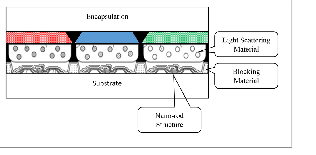
But SDC did not stop there and continued to look for other alternatives, particularly as blue OLED materials are not phosphorescent and inherently generate considerably less light than those that are phosphorescent (red and green).  SDC came up with the idea of using what are known as nano-rods that are essentially very small LED ‘tubes’ that emit blue light.  By substituting these nano-rods for the blue OLED material they were able to overcome the lower light output issue that was present in the alternative technology.
There is a problem however in that such nano-structures must be grown in place, must be vertically oriented, and must have an equal number in each sub-pixel.  If a nano-rod is not vertical it will short other rods and the sub-pixel will fail.  If the number of nano-rods in a pixel is greater or less than required, that sub-pixel will be brighter or darker than the rest, causing non-uniformity, a definite no-no in the display space.  In order to compensate for these issues SDC has had to added ‘electrodes’ that ‘sense’ whether a nano-rod is ‘aligned’ and can also be used to adjust the brightness of the sub-pixel if it has too many or too few nano-rods, but all of these checks and balances add up to complexity, which adds up to cost.
That said, the goal at SDC is to be able to produce a large display that has better overall image quality than current OLED TVs, and according to some, nano-rod based displays fit that bill, however when it comes to displays, there has to be a visible path to large scale production that is cost effective, and while few new display technologies have such a clear view when in the early stages of mass production, there has to be a realistic vision of how long it will take to become viable and profitable.  OLED TV panel production, at current volume levels, is just becoming profitable for LG Display, after almost nine years in production (albeit pilot line production in the early years), so the complexity of SDC’s nano-rod technology must be evaluated in the same way. 
Given that the company has committed significant resources to its development and has allocated dedicated capacity for its production, SDC is certainly willing to give it a chance, and if successful will build out that capacity, but despite those who support  the technology, there is considerable distance between generating the technology on a limited basis and producing a few million or so panels per year, and we likely will not see anything on a commercial level until 2022 to be able to judge both quality and generate a cost curve, although the saying “No guts, no glory” is certainly a valid one in this case.
Picture
Nano-Rod Pixel - Source: SCMR LLC, UBI Research
0 Comments

Apple Revving Up Mini-LED Supply Chain

8/2/2021

0 Comments


Apple Revving Up Mini-LED Supply Chain
​

Late last year we noted that Taiwan based Fittech (6706.TT) had been added to Apple’s (AAPL) supplier list and was expanding their capacity by 3x – 4x, with the expectations that they would complete the expansion early this year.  The company, which provides Mini-LED testing tools indicated in April that it had order visibility through September of this year, and now has noted it has orders for delivery through 1H ’22.  In April FitTech stated that it has received ‘significant’ orders for equipment for probing, testing, and sorting mini-LEDs, which we assumed were from Apple or Apple’s OEMs, which for some of Apple’s expected Mini-LED products are Heesung Electronics (pvt), as the assembler, GIS (6456.TT) as the touch provider, and LG Display (LPL) as the display provider.  While there has been no absolute confirmation of same, much of the talk in the Taiwan trade press seems to indicate that such is the case.
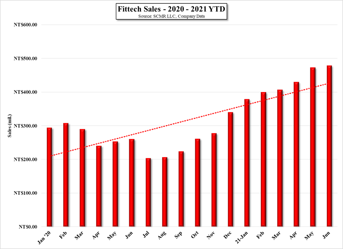
Fittech had indicated that it expected sales of LED sorting, probing, and testing equipment to increase from 20% - 30% of revenue last year to 40% - 50% this year, and is now expecting more than 50% from same, with Mini-LED orders from OEMs at least doubling this year.  While the overall share of LED test, sort, and probe revenue will decrease from almost 80% last year to between 70% and 75% this year as tools for measuring 5G laser and optical functions for 5G and sensing are also growing, monthly revenue through 1H is up 55.9% y/y and set a new company record in 2Q, growing 16.6% q/q and 84.3% y/y.  While we expect not all of the incremental Mini-LED revenue is from Apple, it certainly does not hurt to have become a key equipment supplier to a company at the beginning of a new display modality cycle.
 
Picture
Fittech Sales - 2020 - 2021 YTD - Source: SCMR LLC, Company Data
0 Comments

Samsung OLED TV Update

8/2/2021

0 Comments


Samsung OLED TV Update
​

Way back in 2013 when both Samsung (005930.KS) and LG Electronics (066570.KS) showed OLED TVs at CES, it looked like it was going to be a two-man race for dominance in the space, however in one of the more significant decisions in the display space over the last twenty years, Samsung decided that they would not pursue OLED TV production, citing what it called the inferior quality of the WOLED process and the lack of a cost-effective process for producing OLED TVs using the RGB process.  Samsung remained the biggest proponent of small panel OLED, which uses the RGB FMM (Fine Metal Mask) process to create three color pixels, but left the OLED TV space to rival LG, who is the dominant producer (essentially the only producer) of OLED TV panels.
As we have noted many times, Samsung’s affiliate, Samsung Display is pursuing the development of an alternative process for producing large size OLED TV panels (see above), but is still in the development stage and will likely not begin mass production until next year, and then on a relatively limited basis.But it seems that SDC is not putting all of its eggs in one basket and while working toward the finalization of its QD/OLED project, is exploring another alternative that could change Samsung’s attitude toward OLED TV by allowing it to produce large panel OLED TVs using the FMM process they use when producing small panel RGB OLED displays.
Using fine metal masks to produce small panel OLED displays on Gen 6 fabs works, but while the masks are extremely rigid, when they are used in larger generation fabs, they sag enough that the sub-pixels do not align properly, which has limited their use to Gen 6 fabs or smaller.  That said Samsung and tool supplier Ulvac (6728.JP) have developed a deposition system that rather than sits horizontally (where gravity works against the larger FMM) the deposition system is vertical, which negates the gravitational effect on the fine metal mask, and according to our friends at OLED-A, would allow fine metal masks to be used in a Gen 8.5 OLED fab.
Currently Samsung is evaluating the tool (produced by Ulvac) which would not only allow them to produce RGB OLED large panels but would ween them from deposition tool supplier Canon Tokki (7751.JP) who controls the OLED deposition tool market.  What makes this more interesting, if it pans out, is that the process, which mirrors SDC’s small panel OLED display process, would not require a color filter, which would reduce brightness, would not require quantum dot color conversion, would not require a ‘cut’ process[1], and would likely be cheaper than QD/OLED, and SDC has idle Gen 8.5 capacity that it could more easily convert to such a process than building greenfield lines for other large panel display modalities.
Of course, this is all based on considerable conjecture as the heart of the project, the deposition tool, is under evaluation, and if acceptable, would be quite expensive given its one-off nature.  That said, if, and there are still many potential ‘ifs’, Samsung is able to bypass the FMM issue and is able to produce large panel OLED displays using the RGB process, it will represent a big challenge for LG Display and could be a boon for OLED material suppliers, but we expect that we are still quite far away from this potential process being used in a mass production setting.  That said, it seems that SDC is serious enough to have worked with, and likely funded some of the new tool’s development, and while that does not guarantee its implementation, it certainly gives it a way in a very large door.


[1]   When large OLED panels are produced, while the substrate is Gen 8, the deposition steps require the panel be cut in half or in quarters, which means more expensive deposition tools or slower and therefore more expensive processing.
0 Comments
Forward>>

    Author

    We publish daily notes to clients.  We archive selected notes here, please contact us at: ​[email protected] for detail or subscription information.

    Archives

    May 2025
    April 2025
    March 2025
    February 2025
    January 2025
    January 2024
    November 2023
    October 2023
    September 2023
    August 2023
    June 2023
    May 2023
    February 2023
    January 2023
    December 2022
    November 2022
    October 2022
    September 2022
    August 2022
    July 2022
    June 2022
    May 2022
    April 2022
    March 2022
    February 2022
    January 2022
    December 2021
    November 2021
    October 2021
    September 2021
    August 2021
    July 2021
    June 2021
    May 2021
    April 2021
    March 2021
    February 2021
    January 2021
    December 2020
    October 2020
    July 2020
    May 2020
    November 2019
    April 2019
    January 2019
    January 2018
    August 2017
    July 2017
    June 2017
    May 2017
    April 2017
    March 2017
    February 2017
    January 2017
    November 2016
    October 2016
    September 2016

    Categories

    All
    5G
    8K
    Aapl
    AI
    AMZN
    AR
    ASML
    Audio
    AUO
    Autonomous Engineering
    Bixby
    Boe
    China Consumer Electronics
    China - Consumer Electronics
    Chinastar
    Chromebooks
    Components
    Connected Home
    Consumer Electronics General
    Consumer Electronics - General
    Corning
    COVID
    Crypto
    Deepfake
    Deepseek
    Display Panels
    DLB
    E-Ink
    E Paper
    E-paper
    Facebook
    Facial Recognition
    Foldables
    Foxconn
    Free Space Optical Communication
    Global Foundries
    GOOG
    Hacking
    Hannstar
    Headphones
    Hisense
    HKC
    Huawei
    Idemitsu Kosan
    Igzo
    Ink Jet Printing
    Innolux
    Japan Display
    JOLED
    LEDs
    Lg Display
    Lg Electronics
    LG Innotek
    LIDAR
    Matter
    Mediatek
    Meta
    Metaverse
    Micro LED
    Micro-LED
    Micro-OLED
    Mini LED
    Misc.
    MmWave
    Monitors
    Nanosys
    NFT
    Notebooks
    Oled
    OpenAI
    QCOM
    QD/OLED
    Quantum Dots
    RFID
    Robotics
    Royole
    Samsung
    Samsung Display
    Samsung Electronics
    Sanan
    Semiconductors
    Sensors
    Sharp
    Shipping
    Smartphones
    Smart Stuff
    SNE
    Software
    Tariffs
    TCL
    Thaad
    Tianma
    TikTok
    TSM
    TV
    Universal Display
    Visionox
    VR
    Wearables
    Xiaomi

    RSS Feed

Site powered by Weebly. Managed by Bluehost