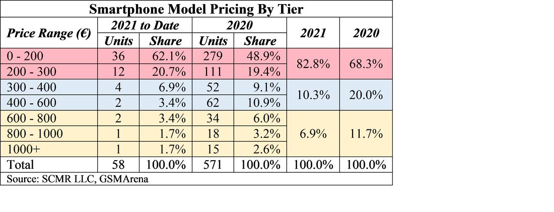
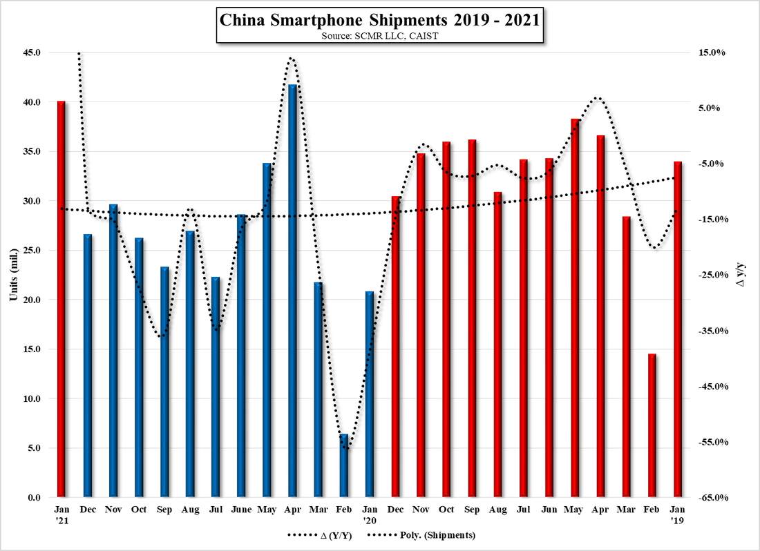
Adding Insult to Injury
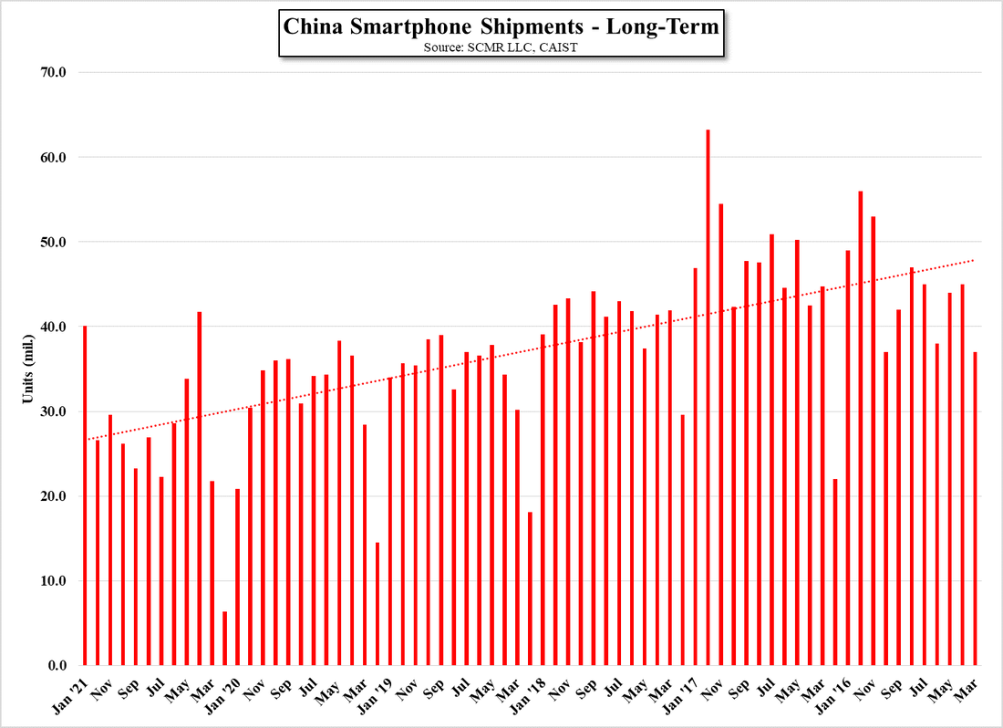
As we noted previously, semiconductor foundry capacity has been constrained and chip shortages have become a topic for consideration in developing estimates in the CE space. Aside from the inherent capacity issues, a number of recent fires at fabs have made the problem worse and now Mother Nature has also come into play as an earthquake of the coast in Japan over the weekend, caused the Renesas (6723.JP) Naki plant to close on Monday so it could be checked for damage and restart procedures begun.
The site of the 7.1 magnitude quake was ~40km north of the Fukushima Daiichi Nuclear Power Plant, the site of the March 11, 2011 earthquake and Tsunami that caused a nuclear meltdown and radioactive particle release. The issue at the Renesas Naki plant was a short power outage, and while the equipment was restarted, it is expected that full production capacity will take at least a week to be restored. This particular fab is the company’s only 12” wafer fab and 28nm process node, which we believe has been focused on automotive semiconductor production, which has been one of the areas that has faced the most constraints in the foundry space.
The site of the 7.1 magnitude quake was ~40km north of the Fukushima Daiichi Nuclear Power Plant, the site of the March 11, 2011 earthquake and Tsunami that caused a nuclear meltdown and radioactive particle release. The issue at the Renesas Naki plant was a short power outage, and while the equipment was restarted, it is expected that full production capacity will take at least a week to be restored. This particular fab is the company’s only 12” wafer fab and 28nm process node, which we believe has been focused on automotive semiconductor production, which has been one of the areas that has faced the most constraints in the foundry space.


 RSS Feed